Revolutionizing Electronics: The Rise of Additive PCB Technology
Key Takeaways
The advent of additive PCB technology is significantly reshaping the landscape of pcb manufacturing. You are likely aware that traditional methods often present challenges such as high costs and lengthy turnaround times, particularly for complex multilayer boards. However, with additive manufacturing techniques, you can experience a remarkable transformation in your pcb manufacturing business. This innovative approach allows for the creation of intricate designs with fewer layers and materials, ultimately reducing both the pcb manufacturing cost and time required to prototype. It empowers you to achieve rapid prototyping, enabling you to iterate designs quickly and efficiently, which is crucial in today’s fast-paced electronics environment. You will find that as more pcb manufacturing companies adopt these methods, they’re not only streamlining their production processes but also enhancing the performance capabilities of high-speed and high-frequency devices. As you explore these developments, keep in mind how they can open new avenues for your projects and push the boundaries of what is possible in electronics design and engineering.
Introduction to Additive PCB Technology
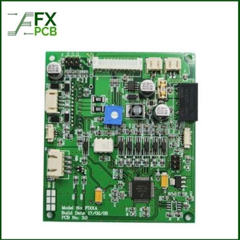
In the ever-evolving landscape of electronics, additive PCB technology represents a transformative shift in how PCB manufacturing is approached. This innovative method stands out by allowing for the creation of intricate multilayer boards with a level of precision that traditional methods struggle to achieve. As you delve into the world of additive manufacturing, you’ll find that this technology streamlines the PCB manufacturing process, reducing the time from design to production while significantly enhancing flexibility.
Many PCB manufacturing companies are beginning to adopt these techniques not only for rapid prototyping—which allows for quicker iterations and adjustments—but also for the overall decrease in PCB manufacturing costs associated with material waste reduction. This is particularly important as you look to optimize your own PCB manufacturing business; better resource management can make a considerable difference in your bottom line.
Furthermore, examining how it integrates into existing production lines can provide valuable insights. For instance, additive processes can be incorporated into the initial stages of design and testing, which leads to maximized efficiency and lower costs overall. Through this lens, your understanding of the electronics sector will deepen as you grasp how additive PCB technologies are setting new standards in performance and capability across various applications.
Advantages of Additive PCB in Electronics Manufacturing
The advent of additive PCB technology has significantly changed the landscape of electronics manufacturing, offering numerous advantages that enhance production efficiency and product quality. One of the most notable benefits is the capacity for rapid prototyping, which allows you to create complex multilayer boards in a fraction of the time compared to traditional methods. This is particularly useful for PCB manufacturing companies looking to innovate quickly, enabling you to respond faster to market demands and reduce the time-to-market for new products. Additionally, by utilizing additive manufacturing techniques, you can see a substantial reduction in PCB manufacturing costs, as fewer materials are wasted and the need for extensive tooling is minimized. This cost efficiency can be a game-changer for your PCB manufacturing business, allowing for more competitive pricing without sacrificing quality. Furthermore, additive technology facilitates the production of high-speed and high-frequency devices, ensuring that your products meet ever-increasing performance standards. In sum, adopting additive PCB technology not only streamlines processes but also enhances overall operational flexibility and innovation potential in the electronics sector.
The Process of Rapid Prototyping with Additive PCBs
The integration of additive PCB technology into the realm of electronics has brought about a notable evolution in the way rapid prototyping operates. This method enables you to create intricate multilayer boards with unprecedented speed and accuracy, thereby streamlining the pcb manufacturing process. As you navigate through the various stages of prototype development, you will find that traditional techniques often introduce delays and complexity. In contrast, additive methods allow for quicker turnaround times and minimal material wastage, key factors that enhance your overall production efficiency.
By using additive manufacturing techniques, your projects can move from conceptualization to a working prototype in a fraction of the time. This is especially crucial when collaborating with various pcb manufacturing companies, as they strive to meet tight deadlines without compromising on quality. Furthermore, as you experiment with complex designs, you’ll see how these innovative methods can support variations that traditional approaches might struggle to accommodate.
It’s important to be mindful that pcb manufacturing cost can spike with changes in design specifications, but with additive technology significantly reducing material requirements and production time, it ultimately provides a more cost-effective solution in the long run. By taking advantage of rapid prototyping solutions offered by this technology, you position your pcb manufacturing business for greater flexibility and responsiveness in an ever-evolving market.
“Incorporating rapid prototyping into your development cycle is not just an option; it’s a strategic advantage that can set your projects apart.”
Adopting this forward-thinking approach allows you to meet clients’ demands swiftly while continuously innovating designs that push the boundaries of what’s currently achievable in electronics. It’s clear that the transformative impact of additive PCB technology on rapid prototyping is not just about speed; it’s also about unlocking potential that drives progress within the industry.
Reducing Costs Through Additive Manufacturing Techniques
One of the most compelling aspects of additive PCB technology is its potential to significantly reduce pcb manufacturing costs. Traditional pcb manufacturing methods often require extensive initial investments in equipment and materials, as well as a lengthy setup process. In contrast, additive manufacturing simplifies the workflow, allowing you to create highly complex multilayer boards with less material waste. As a result, many pcb manufacturing companies are increasingly adopting these technologies to enhance productivity while minimizing expenses. By streamlining production processes and enabling quicker design iterations, you not only decrease downtime but also foster a more agile pcb manufacturing business model. This efficiency is particularly critical in today’s fast-paced electronics market where rapid prototyping is key to staying competitive. Ultimately, as you explore additive methods for PCB production, you’ll find that the cost-saving benefits extend beyond just materials; they include labor and logistical savings as well—further reinforcing the appeal of this innovative approach in your decision-making process regarding PCB production strategies.
Enhancing Performance for High-Speed and High-Frequency Devices
The demand for enhanced performance in high-speed and high-frequency devices is driving innovation in additive PCB technology. As you delve into the realm of pcb manufacturing, you’ll notice how the flexibility and precision offered by this method allows for the creation of complex multilayer boards that traditional methods cannot efficiently achieve. This is particularly important in applications where signal integrity and reduced electromagnetic interference are paramount. By leveraging additive manufacturing techniques, pcb manufacturing companies can create designs that not only minimize the size of components but also maximize performance, leading to improved operational capabilities in devices such as smartphones, routers, and advanced sensors.
What stands out with additive processes is their ability to significantly reduce pcb manufacturing cost while ensuring high reliability. As you explore various options for your pcb manufacturing business, focusing on additive methods can open doors to realizing intricate designs that support faster transmission speeds and better overall efficiency. This technology enables you to prototype rapidly, allowing for quick iterations that cater to evolving design requirements without the significant delays often associated with conventional production methods. In this way, additive PCB technology is not merely a trend but a substantial shift toward meeting the rigorous demands of modern electronics, ensuring that your products remain competitive in a fast-paced market.
Case Studies: Success Stories in Additive PCB Implementation
Additive PCB technology has shown remarkable potential through various case studies that highlight successful implementations in diverse industries. One notable example involves a leading PCB manufacturing company that embraced additive methods to streamline their pcb manufacturing processes. This company faced challenges with traditional pcb manufacturing cost, particularly when aiming to develop intricate multilayer boards for high-performance applications. By transitioning to additive techniques, they achieved not only a significant reduction in production time but also enhanced design flexibility. As a result, they could create complex geometries that were previously unfeasible.
Another inspiring case comes from the telecommunications sector, where a prominent pcb manufacturing business utilized additive PCB technology to respond quickly to market demands for smaller, higher-speed devices. This company leveraged rapid prototyping capabilities, allowing them to test and iterate on designs swiftly. Their ability to reduce lead times contributed significantly to their competitive edge in the high-frequency devices market.
Furthermore, a startup focused on consumer electronics adopted additive PCB methods specifically for prototype development. By doing so, they minimized their experimental costs while enabling innovative features in their products — attributes that resonated well with early adopters and significantly increased their market presence.
These success stories exemplify how businesses can strategically implement additive PCB technology, demonstrating its potential not only in enhancing performance and reducing costs but also in fostering innovation within the ever-evolving electronics landscape.
Future Trends in Additive PCB Technology
As you look to the future of additive PCB technology, several emerging trends promise to reshape the landscape of PCB manufacturing. One notable direction is the increase in automation and digitalization in the production process, allowing PCB manufacturing companies to streamline operations and enhance precision. This shift will likely make it easier for you to navigate complexities in design, particularly with multilayer boards, enabling faster turnaround times while maintaining high quality. Additionally, advancements in materials science are leading to new substrates and conductive inks which can significantly lower PCB manufacturing costs while improving performance characteristics of high-speed and high-frequency devices. As the demand for smaller and lighter electronic components grows, techniques such as 3D printing within the PCB manufacturing business will gain more traction, allowing for complex geometries that conventional methods cannot achieve. Furthermore, environmental considerations are pushing companies towards sustainable practices; consequently, we can expect an increased focus on eco-friendly materials and recycling processes within the additive PCB manufacturing processes. These trends will not only advance production capabilities but also enhance overall sustainability in electronics manufacturing, positioning you to take advantage of a more efficient future in the electronics industry.
Conclusion: The Impact of Additive PCBs on the Electronics Industry
In today’s fast-paced world of electronics, additive PCB technology has undoubtedly become a game changer. You may find that this innovative approach to PCB manufacturing allows you to create complex multilayer boards with remarkable efficiency. As you explore this technology, you will discover that it not only streamlines the prototyping process but also significantly reduces the PCB manufacturing cost, enabling more companies to innovate without overwhelming financial burdens.
For those venturing into the PCB manufacturing business, understanding the advantages offered by additive techniques can enhance your competitive edge. Unlike traditional methods that may waste materials, additive processes use only the necessary amount of resources, making them more environmentally friendly and cost-effective in the long run. Moreover, the rapid prototyping capabilities of additive PCB allow you to quickly test and iterate designs, proving crucial in developing high-speed and high-frequency devices that meet today’s demanding performance benchmarks.
As you assess your options within various PCB manufacturing companies, recognizing the transformative potential of additive technology will position you well in an industry that increasingly values speed and agility. The future looks bright as this technology continues to evolve, fostering a culture of innovation that empowers engineers and manufacturers alike to push boundaries and explore uncharted territories in electronics design.
Conclusion: The Impact of Additive PCBs on the Electronics Industry
As you reflect on the transformative power of additive PCB technology in the electronics sector, consider how these advancements are significantly reshaping pcb manufacturing processes. The rise of this innovative approach optimizes production practices, allowing pcb manufacturing companies to achieve faster turnaround times and greater design flexibility. You might find it intriguing that by embracing additive techniques, businesses can slash the pcb manufacturing cost associated with traditional methods while developing complex multilayer boards that were once challenging to produce. This shift not only enhances operational efficiency but also fosters creativity in design, allowing your projects to push the boundaries of what is achievable in high-speed and high-frequency devices. Ultimately, as you explore the implications of this technology for your own pcb manufacturing business, it’s clear that the adoption of additive PCBs signifies a new era in electronics, where agility and innovation are paramount in meeting consumer demands and advancing technological capabilities.
FAQs
What is additive PCB technology?
Additive PCB technology refers to a modern manufacturing approach that builds printed circuit boards (PCBs) layer by layer, allowing for the creation of complex multilayer boards efficiently.
How does additive manufacturing reduce PCB manufacturing costs?
By minimizing material waste and speeding up the prototyping process, additive manufacturing lowers the overall PCB manufacturing cost, making it more economical for PCB manufacturing companies.
What are the benefits of using additive PCBs in high-speed devices?
Additive PCBs enhance performance for high-speed and high-frequency devices by enabling more intricate designs and smoother signal pathways, thereby improving overall device efficiency.
Can I find case studies that highlight successful additive PCB implementations?
Yes, many PCB manufacturing companies share successful case studies showcasing how they adopted additive PCB technology, demonstrating significant improvements in production capabilities.
What are some future trends in additive PCB technology?
Future trends include increased automation, enhanced materials for improved performance, and broader applications in the electronics sector, further shaping the landscape of PCB manufacturing business practices.
For more information on PCB manufacturing, please click here: Andwin PCB Manufacturing