Revolutionizing Technology: The Art and Science of Assembled Printed Circuit Boards
Key Takeaways
The realm of pcb assembly represents a significant milestone in the evolution of electronics, underscoring the intricate relationship between design and functionality. With each advancement, pcba processes have incorporated more sophisticated methodologies that not only enhance production efficiency but also pave the way for innovations in electronic devices. Key to this evolution is the integration of technology—from automated machinery to advanced soldering techniques—that ensures reliability and precision in every assembled unit. As industries strive for higher performance standards, emphasis on quality control throughout the pcb assembly process becomes paramount. This focus not only addresses production challenges but also guarantees that the end products meet the rigorous demands of modern electronics. A deeper understanding of these methodologies allows professionals to appreciate how each component within a printed circuit board contributes to its overall functionality and reliability, solidifying assembled printed circuit boards as indispensable elements in today’s technology-driven landscape. By staying informed about emerging trends and materials used in pcba, stakeholders can effectively navigate the complexities of this dynamic sector and foster innovation that aligns with future technological needs.
The Evolution of Printed Circuit Boards: A Historical Perspective
The journey of printed circuit boards (PCBs) dates back to the early 20th century, marking a significant turning point in the evolution of electronic devices. The first recognizable form of a PCB emerged in the 1930s when engineer Paul Eisler invented a technique for employing printed circuits in radios. This innovative method streamlined the assembly process, reducing the complexity of wiring, and effectively set the stage for what would become pcb assembly as we know it today. Over subsequent decades, advancements in technology and materials enabled manufacturers to develop more efficient and cost-effective processes for pcba production. The introduction of multi-layer PCBs allowed for greater circuit density, paving the way for compact electronic devices that dominate today’s marketplace.
During the 1960s and 1970s, the burgeoning space industry and consumer electronics’ demands spurred rapid innovation. As techniques improved, quality control mechanisms were integrated to ensure reliability and performance in PCB production. The emergence of automated assembly lines further revolutionized pcba methods, making it possible to meet escalating production demands while maintaining high precision.
“Understanding the historical context of PCBs underscores their critical role in transforming modern electronics,” reflects industry expert James T. “By appreciating this evolution, we can better anticipate future advancements.”
As we look back on these developments, it’s clear that assembled printed circuit boards have not only facilitated technological advancements but have also laid a robust foundation for future innovations across various sectors.
Understanding the PCB Design Process: From Concept to Prototype
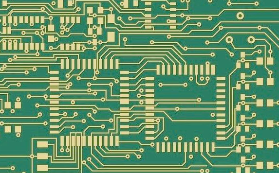
The process of PCB design typically begins with an initial concept that outlines the functional requirements of the intended electronic device. Designers utilize specialized software tools to create schematics, which represent the electrical connections and components. Once the schematics are finalized, it transitions into creating a physical layout—this is where pcb assembly begins to take shape. The layout must consider factors such as size, component placement, and electrical performance to ensure optimal functionality in the final product.
Following this, a prototype is developed, allowing engineers to verify that the design performs as expected in real-world conditions. This stage often involves iterative testing and refinement, as adjustments may be needed based on prototypes’ behaviors. Important considerations include ensuring effective signal integrity and power distribution within the board.
As part of this journey, understanding pcba (printed circuit board assembly) techniques becomes crucial. These techniques influence how components are mounted on the board—be it through traditional through-hole methods or more modern surface-mount technology (SMT). Selecting advanced materials that enhance thermal management and durability can significantly elevate both the performance and reliability of assembled printed circuit boards.
Ultimately, this intricate design process underscores the essential role of pcba in transitioning from abstract ideas to functioning prototypes, solidifying how significant these boards are in technological development today. The efficiency gained here lays a foundation for innovations across various industries reliant on electronic components.
Cutting-Edge Techniques in PCB Assembly: Innovations and Methodologies
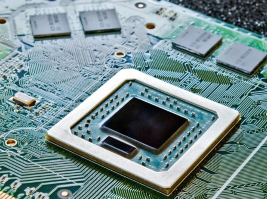
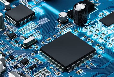
In the dynamic field of pcb assembly, various cutting-edge techniques and methodologies have emerged, enabling manufacturers to push the boundaries of what is possible in printed circuit board assembly (PCBA). These advancements are characterized by a blend of sophisticated automation, precision placement technologies, and innovative design software. One key innovation is the use of surface mount technology (SMT), which allows components to be mounted directly onto the surface of the PCB, thus maximizing space efficiency and enabling more complex circuit designs. Furthermore, advanced pick-and-place machines have significantly improved speed and accuracy in component placement, reducing human error and enhancing overall production efficiency.
Another noteworthy development is the integration of robotics into the PCB assembly process. Automated systems equipped with artificial intelligence are now capable of performing intricate tasks such as soldering and inspection. This not only increases productivity but also contributes to consistent quality control, which is essential for ensuring that assembled boards meet rigorous performance specifications. Additionally, techniques such as multi-layer PCB assembly allow for enhanced functionality within smaller form factors, aligning with the growing demand for compact electronic devices.
Moreover, the role of advanced materials in pcba cannot be understated. The introduction of high-frequency laminates and flexible substrates has revolutionized how printed circuit boards function in various applications—from telecommunications to consumer electronics—offering improved durability and performance under diverse conditions. The convergence of these leading-edge technologies highlights a significant trend where innovation meets necessity in addressing contemporary challenges within electronics manufacturing.
As these cutting-edge techniques continue to evolve, they not only enhance manufacturing processes but also pave the way for new applications and products that further integrate technology into everyday life. This transformative journey in pcb assembly underscores its vital role in shaping both the present landscape and future vision of global electronics industries.
Quality Control in PCB Production: Ensuring Reliability and Performance
Quality control in PCB production is a critical step that ensures the reliability and performance of assembled printed circuit boards (PCBA). This meticulous process begins with rigorous inspection at various stages of pcb assembly, from the initial design to the final manufactured product. Implementing systematic quality assurance measures helps to identify potential defects early in the production line, thus minimizing waste and ensuring that only the highest quality products reach consumers.
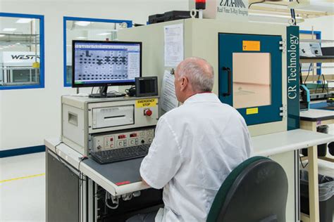
Among the essential methods of quality control are Automated Optical Inspection (AOI) and X-ray inspection, both of which provide detailed assessments of solder joints and component placements. These technologies are vital for detecting issues that are invisible to the naked eye, such as latent defects in multilayer boards. The table below illustrates some common quality control methods employed in pcb assembly:
| Quality Control Method | Description |
|---|---|
| Automated Optical Inspection | Utilizes cameras to scan PCBs, identifying defects by comparing them against a defined model. |
| X-ray Inspection | Allows for internal inspection of multilayer boards, revealing faults not accessible through surface checks. |
| Functional Testing | Ensures that assembled boards operate according to specified performance criteria under real-world conditions. |
| In-Circuit Testing | Verifies the integrity of individual components on the PCB by measuring their electrical properties during assembly. |
Adopting a proactive approach to quality control not only guarantees exceptional product performance but also fosters consumer trust in electronic devices reliant on these intricate components. The integration of advanced methodologies and technologies reinforces an industry’s commitment to delivering reliable electronic solutions, ultimately shaping future innovations within diverse sectors.
The Role of Advanced Materials in Enhancing PCB Functionality
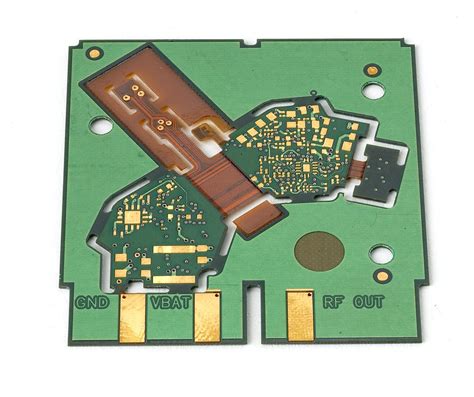
The landscape of pcb assembly has witnessed transformative changes, largely driven by the advent of advanced materials that significantly enhance the functionality and durability of printed circuit boards (PCBs). These materials, which include high-frequency laminates, flexible substrates, and heat-resistant composites, are meticulously engineered to meet the demands of modern electronics. For instance, the utilization of high-frequency laminates allows for greater signal integrity in RF applications, while flexible substrates enable innovative designs in compact and wearable technology. Additionally, incorporating heat-resistant composites ensures that PCBs can withstand harsh operating environments without compromising performance. The ongoing innovation in material science not only improves the reliability and lifespan of PCBs but also plays a crucial role in reducing production costs associated with pcba processes. Furthermore, the strategic use of these materials facilitates miniaturization and integration of components, pushing boundaries in design capabilities and opening doors to new applications across various industries. This synergy between advanced materials and PCB functionality draws a direct link to enhanced performance metrics in final electronic products, underscoring the importance of continuous research and development within this field.
Overcoming Production Challenges in Assembled Circuit Boards
In the realm of pcb assembly, various production challenges can arise that threaten the efficiency and efficacy of the manufacturing process. A critical aspect of successful pcba lies in understanding these obstacles and developing strategies to address them effectively. One prominent issue is maintaining the integrity of the components throughout assembly; even slight misalignments can lead to performance failures. To combat this, manufacturers often implement advanced alignment technologies that enhance precision during placement, ensuring that each component is positioned correctly on the printed circuit board.
Additionally, managing the thermal stresses associated with soldering processes is essential, as excessive heat can compromise component durability and functionality. Employing innovative materials with superior thermal properties can mitigate these risks, allowing for a smoother assembly process without sacrificing quality. Lastly, contamination control remains a significant challenge; any foreign particles can lead to defects in the final product. Implementing rigorous cleaning protocols and utilizing sealed environments help manufacturers maintain high-level cleanliness standards throughout production.
By addressing these issues through continual improvement and leveraging modern technologies, companies involved in pcb assembly can overcome production challenges, thereby reinforcing their position within the competitive electronics industry landscape. In doing so, they not only enhance their overall productivity but also contribute significantly to the reliability of electronic devices globally.
Future Trends in PCB Technology: Shaping the Electronics Industry
As we look towards the horizon of PCB technology, several trends are anticipated to significantly shape the future of the electronics industry. One such trend is the increased integration of smart technologies into the process of PCB assembly. The advent of Internet of Things (IoT) devices is pushing manufacturers to design printed circuit boards that are not only compact but also capable of communicating wirelessly. Furthermore, advancements in automated assembly techniques are streamlining production processes, resulting in higher efficiency and lower costs. Innovations in materials play a crucial role as well; lightweight but durable substances are being utilized to create PCBA that can withstand harsh environments while ensuring optimal performance. Additionally, sustainability is becoming a focal point, leading to a push for eco-friendly manufacturing practices and recyclable materials in PCB design. This convergence of technology, materials science, and environmental responsibility appears set to redefine industry standards and pave the way for smarter, more efficient electronic components in various applications from consumer gadgets to intricate aerospace systems. Each development in pcb assembly not only elevates product reliability but also fuels further exploration into what is possible within electronic systems, creating a robust foundation for continued innovation in this dynamic field.
The Impact of Assembled Printed Circuit Boards on Global Markets
The significance of assembled printed circuit boards (PCBs) in driving economic growth cannot be overstated. As industries increasingly rely on pcb assembly for electronic devices, the demand for high-quality pcba has surged, prompting manufacturers to innovate and adapt. The integration of advanced technologies in pcb assembly processes not only enhances the efficiency of production but also contributes to the overall reliability and performance of electronic components. This increasing demand reflects broader trends in consumer electronics, automotive technology, and telecommunications, where improved connectivity and functionality are vital.
Additionally, regions specializing in pcba production have witnessed substantial economic benefits. By cultivating a skilled workforce knowledgeable in cutting-edge PCB assembly techniques, these areas have positioned themselves as integral players on the global stage. The evolution towards more complex and efficient assembled printed circuit boards has also resulted in the establishment of international partnerships, fostering collaboration across borders. As a result, companies focusing on high-quality pcb assembly are not only enhancing their market share but are also contributing to a more dynamic global market landscape.
Overall, it is evident that assembled printed circuit boards play a crucial role in shaping economic trends worldwide. Their impact extends beyond mere functionality; it influences innovation cycles and sets a foundation for future advancements across various sectors. The continual evolution of pcba technology is set to further transform industries and contribute positively to global economic growth, illustrating that these components are not just parts but essential elements driving progress forward.
Conclusion
In the rapidly evolving landscape of electronics, the importance of pcb assembly cannot be overstated. As we have explored, the meticulous process of assembling printed circuit boards, or PCBA, is foundational to creating efficient and reliable electronic devices. The intersection of advanced technologies, innovative techniques, and rigorous quality control measures results in PCB designs that can outperform traditional methods. As we move forward, embracing cutting-edge materials and processes will only enhance the performance and durability of assembled circuit boards. Furthermore, understanding the global implications of these advancements is crucial for companies aiming to maintain a competitive edge in the market. The continuous evolution in this field not only promises to enhance functionality but also to drive significant shifts in how we approach electronic design and manufacturing. Ultimately, the art and science behind assembled printed circuit boards is not just about creating components; it’s about shaping the future of technology itself.
FAQs
Understanding pcb assembly can raise numerous questions for both industry professionals and enthusiasts alike. One frequently asked question is: What are the main steps involved in the pcb assembly process? The process generally starts with the design and layout of the printed circuit board, where engineers utilize specialized software to create schematics and PCB blueprints. Following this, the fabrication stage produces the bare boards, which are then sent to assembly. Here, components are carefully placed on the board using methods such as surface-mount technology (SMT) or through-hole technology, ensuring each component is accurately positioned for optimal functionality.
Another common inquiry pertains to quality control measures within pcb assembly processes. Quality assurance is crucial in ensuring that assembled PCBs meet established standards and perform reliably in their intended applications. Testing methods such as Automated Optical Inspection (AOI) and Functional Testing are typically employed to identify defects early and maintain rigorous quality standards.
Additionally, many wonder about the impact of advanced materials on pcba capabilities. Innovative materials can enhance thermal management, electrical performance, and mechanical durability of assembled circuit boards, making them crucial for meeting the evolving demands of modern technology.
For comprehensive insights into these topics and more regarding assembled printed circuit boards, please explore further resources specializing in PCB solutions.