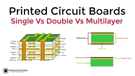
Rf pcb design rules
Importance Of Impedance Matching In RF PCB Design
In the realm of radio frequency (RF) printed circuit board (PCB) design, the concept of impedance matching holds paramount importance. As RF circuits operate at high frequencies, typically ranging from a few megahertz to several gigahertz, the challenges associated with signal integrity and transmission line effects become significantly pronounced. Impedance matching, therefore, emerges as a critical design consideration to ensure optimal performance and efficiency of RF circuits.
To begin with, impedance matching is essential for minimizing signal reflections that occur when there is a mismatch between the source impedance,
the transmission line, and the load impedance. These reflections can lead to standing waves, which not only degrade signal quality but also result in power loss. By carefully matching the impedances, designers can ensure that the maximum amount of power is transferred from the source to the load, thereby enhancing the overall efficiency of the RF system. This is particularly crucial in applications such as wireless communication, where signal integrity is vital for maintaining reliable data transmission.
Moreover, impedance matching plays a significant role in reducing electromagnetic interference (EMI) and crosstalk between adjacent traces on a PCB.
In high-frequency circuits, even small discontinuities in impedance can act as sources of EMI, potentially affecting the performance of nearby components. By maintaining consistent impedance throughout the transmission path, designers can mitigate these unwanted emissions, thereby improving the electromagnetic compatibility (EMC) of the device. This is especially important in densely packed PCBs, where space constraints necessitate close proximity of traces and components.
In addition to minimizing reflections and EMI, impedance matching is crucial for maintaining the bandwidth of RF circuits.
A mismatch in impedance can lead to a reduction in bandwidth, limiting the range of frequencies over which the circuit can operate effectively. This can be particularly detrimental in applications such as broadband communication systems, where wide bandwidth is essential for accommodating multiple channels and high data rates. By ensuring proper impedance matching, designers can preserve the bandwidth and, consequently, the performance of the RF system.
Furthermore, impedance matching is integral to the design of RF filters and amplifiers, which are commonly used in RF circuits to select desired frequencies and boost signal strength.
In these components, impedance matching is necessary to achieve the desired frequency response and gain characteristics. For instance, in RF amplifiers, a mismatch can lead to reduced gain and increased noise figure, adversely affecting the signal-to-noise ratio. Similarly, in RF filters, impedance mismatches can result in unwanted passband ripple and poor out-of-band rejection.
In conclusion, the importance of impedance matching in RF PCB design cannot be overstated. It is a fundamental aspect that influences various performance parameters, including signal integrity, power transfer, EMI, bandwidth, and component functionality. As RF technology continues to advance and find applications in diverse fields such as telecommunications, aerospace, and consumer electronics, the need for precise impedance matching becomes even more critical. By adhering to established design rules and employing advanced simulation tools, designers can effectively address the challenges associated with impedance matching, thereby ensuring the successful implementation of RF circuits in modern electronic systems.
Techniques For Minimizing Signal Loss In RF PCB Layout
In the realm of radio frequency (RF) printed circuit board (PCB) design, minimizing signal loss is a critical objective that demands meticulous attention to detail and a comprehensive understanding of the underlying principles. Signal loss in RF circuits can significantly degrade performance, leading to inefficiencies and potential failures in communication systems. Therefore, employing effective techniques to mitigate these losses is paramount for engineers and designers.
One of the primary considerations in minimizing signal loss is the selection of appropriate materials.
The dielectric material used in the PCB substrate plays a crucial role in determining the signal integrity. Low-loss dielectric materials, such as PTFE (polytetrafluoroethylene) or Rogers materials, are often preferred due to their favorable electrical properties, including low dielectric constant and low dissipation factor. These materials help reduce dielectric losses, which are a significant contributor to overall signal attenuation.
In addition to material selection, the layout of the RF traces is another critical factor.
The width and spacing of these traces must be carefully calculated to maintain the characteristic impedance, typically 50 ohms, which is standard for most RF applications. Impedance mismatches can lead to reflections and standing waves, exacerbating signal loss. Utilizing microstrip or stripline configurations can help achieve the desired impedance while minimizing radiation losses.
Moreover, the use of ground planes is essential in RF PCB design.
A continuous ground plane beneath the RF traces provides a return path for the signals, reducing inductive and capacitive coupling with other circuit elements. This configuration not only minimizes electromagnetic interference (EMI) but also enhances signal integrity by reducing the loop area, which is a common source of radiated emissions.
Transitioning to the topic of via design, it is important to note that vias can introduce parasitic inductance and capacitance, which can adversely affect signal performance.
To mitigate these effects, designers should minimize the number of vias in the RF path and ensure that any necessary vias are adequately back-drilled or filled to reduce their impact. Additionally, using blind or buried vias can help maintain signal integrity by reducing the length of the signal path through the via.
Furthermore, the placement of components on the PCB can significantly influence signal loss.
Components should be strategically positioned to minimize the length of RF traces, thereby reducing resistive losses. It is also advisable to place sensitive components away from high-power or noisy sections of the circuit to prevent unwanted coupling and interference.
Another technique to consider is the use of proper termination and matching networks.
These networks are crucial for ensuring that the load impedance matches the source impedance, thereby minimizing reflections and maximizing power transfer. Implementing matching networks using components such as capacitors, inductors, and transmission lines can effectively reduce signal loss and improve overall circuit performance.
Finally, thermal management should not be overlooked in RF PCB design.
Excessive heat can increase resistive losses and degrade the performance of components. Therefore, incorporating thermal vias, heat sinks, and appropriate copper thickness can help dissipate heat efficiently, maintaining the integrity of the RF signals.
In conclusion, minimizing signal loss in RF PCB layout requires a holistic approach that encompasses material selection, trace layout, via design, component placement, and thermal management. By adhering to these techniques, designers can significantly enhance the performance and reliability of RF circuits, ensuring optimal functionality in a wide range of applications.
Best Practices For Ground Plane Design In RF PCBs
In the realm of RF PCB design, the ground plane plays a pivotal role in ensuring optimal performance and signal integrity. As RF circuits operate at high frequencies, any imperfections in the ground plane can lead to significant issues such as signal loss, interference, and unwanted radiation. Therefore, adhering to best practices in ground plane design is essential for achieving reliable and efficient RF PCB performance.
To begin with, one of the fundamental principles in ground plane design is maintaining a continuous and unbroken plane.
This continuity is crucial because any gaps or breaks can create impedance discontinuities, which in turn can cause signal reflections and degrade the performance of the RF circuit. To avoid such issues, designers should ensure that the ground plane is as solid and uninterrupted as possible, especially beneath critical components and transmission lines.
Moreover, it is important to consider the placement of vias in the ground plane.
Vias are necessary for connecting different layers of a PCB, but they can also introduce inductance and disrupt the current flow if not placed strategically. To mitigate these effects, designers should use multiple vias to create a low-inductance path and place them close to the signal vias. This practice helps in maintaining a low impedance return path, which is vital for minimizing electromagnetic interference (EMI) and ensuring signal integrity.
In addition to via placement, the proximity of the ground plane to the signal traces is another critical factor.
Ideally, the ground plane should be placed as close as possible to the signal layer to form a microstrip or stripline configuration. This close proximity helps in reducing the loop area, thereby minimizing the inductance and enhancing the coupling between the signal and ground. Consequently, this configuration aids in reducing radiation and improving the overall performance of the RF circuit.
Furthermore, designers should pay attention to the concept of grounding in RF PCB design.
A common practice is to use a single-point ground or a star ground configuration to prevent ground loops, which can introduce noise and degrade the performance of the circuit. By connecting all ground points to a single reference point, designers can ensure a stable and noise-free ground system.
Another best practice involves the use of ground stitching vias around the perimeter of the PCB and near the edges of the ground plane.
These stitching vias help in containing the electromagnetic fields within the PCB and prevent them from radiating outwards. This containment is particularly important in RF designs, where minimizing EMI is crucial for compliance with regulatory standards and for preventing interference with other electronic devices.
Finally, thermal management should not be overlooked in ground plane design.
The ground plane can serve as a heat sink, dissipating heat away from critical components. Therefore, designers should ensure that the ground plane is adequately sized and connected to thermal vias to facilitate efficient heat dissipation.
In conclusion, the design of the ground plane in RF PCBs is a critical aspect that requires careful consideration and adherence to best practices. By ensuring continuity, strategic via placement, close proximity to signal traces, effective grounding, and proper thermal management, designers can significantly enhance the performance and reliability of RF circuits. These practices not only help in achieving optimal signal integrity but also in minimizing EMI, thereby ensuring that the RF PCB meets the desired performance criteria and regulatory standards.
Strategies For Effective RF Shielding In PCB Design
In the realm of printed circuit board (PCB) design, particularly for radio frequency (RF) applications, effective RF shielding is paramount to ensure optimal performance and reliability. As electronic devices become increasingly compact and complex, the need for robust RF shielding strategies has never been more critical. This article delves into the essential strategies for achieving effective RF shielding in PCB design, providing insights into the techniques and considerations that can significantly enhance the performance of RF circuits.
To begin with, understanding the fundamental purpose of RF shielding is crucial.
RF shielding is employed to prevent electromagnetic interference (EMI) from affecting the performance of electronic components. This interference can originate from both external sources and internal components within the PCB itself. Therefore, the primary goal of RF shielding is to isolate sensitive components from these unwanted signals, thereby maintaining signal integrity and reducing noise.
One of the most effective strategies for RF shielding is the use of ground planes.
Ground planes serve as a reference point for all signals on the PCB and provide a low-impedance path for return currents. By strategically placing ground planes adjacent to signal layers, designers can create a natural barrier that minimizes the coupling of RF signals between different parts of the circuit. Moreover, ground planes can be connected to the chassis ground, further enhancing their shielding effectiveness.
In addition to ground planes, the implementation of shielding enclosures is another vital strategy.
These enclosures, often made of conductive materials such as metal, physically encase sensitive components, preventing external RF signals from penetrating the enclosure and interfering with the circuit. When designing shielding enclosures, it is essential to consider factors such as material selection, thickness, and the presence of any apertures or openings, as these can significantly impact the shielding effectiveness.
Furthermore, the careful routing of traces is a critical aspect of RF shielding in PCB design.
Traces should be kept as short as possible to reduce the potential for RF interference. Additionally, maintaining adequate spacing between traces and ensuring that they are routed perpendicular to each other can help minimize crosstalk and coupling. It is also advisable to avoid routing traces over split ground planes, as this can create impedance discontinuities and degrade signal integrity.
Another important consideration is the use of decoupling capacitors.
These components are placed near power supply pins to filter out high-frequency noise and provide a stable voltage supply to the circuit. By selecting appropriate values and placing them strategically, decoupling capacitors can significantly enhance the overall RF shielding effectiveness of the PCB.
Moreover, the choice of materials used in the PCB itself can influence RF shielding.
High-frequency laminates with low dielectric constants and loss tangents are preferred for RF applications, as they help maintain signal integrity and reduce losses. Additionally, the use of via stitching, which involves placing vias around the perimeter of a shielded area, can improve the grounding and further enhance the shielding effectiveness.
In conclusion, effective RF shielding in PCB design is a multifaceted challenge that requires careful consideration of various strategies and techniques. By employing ground planes, shielding enclosures, meticulous trace routing, decoupling capacitors, and appropriate material selection, designers can significantly mitigate the impact of electromagnetic interference on RF circuits. As technology continues to advance, the importance of robust RF shielding strategies will only grow, underscoring the need for designers to remain vigilant and innovative in their approach to PCB design.