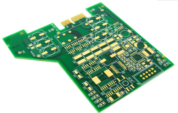
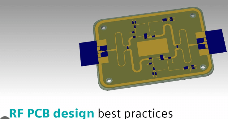
Rf pcb design tutorial
Top Features To Look For In RF PCB design tutorial.
When selecting RF PCB design software, it is crucial to consider several key features that can significantly impact the efficiency and accuracy of your design process. One of the primary aspects to evaluate is the software’s ability to handle high-frequency signals. RF circuits operate at frequencies where even minor design flaws can lead to significant performance degradation. Therefore, the software must offer robust simulation tools that can accurately predict the behavior of RF signals, ensuring that the final product meets the desired specifications.
Another essential feature to look for is the software’s layout capabilities.
RF PCB design requires meticulous attention to detail, particularly in the placement and routing of components. The software should provide advanced layout tools that facilitate precise component placement and routing, minimizing signal interference and loss. Additionally, it should support various design rules and constraints specific to RF circuits, such as controlled impedance routing and differential pair routing, to ensure optimal performance.
Integration with other design tools is also a critical factor.
RF PCB design is often part of a larger system design process, which may involve multiple software tools for different aspects of the project. The ability to seamlessly integrate with other design tools, such as schematic capture, signal integrity analysis, and thermal analysis software, can streamline the design process and reduce the likelihood of errors. This integration can also facilitate collaboration among team members, allowing for more efficient and effective design iterations.
Furthermore, the software should offer comprehensive library support.
Access to a vast library of components, including RF-specific components such as filters, amplifiers, and antennas, can significantly expedite the design process. The library should also be regularly updated to include the latest components and technologies, ensuring that designers have access to the most current options available.
User-friendliness is another important consideration.
The software should have an intuitive interface that allows designers to quickly and easily navigate through the various tools and features. This ease of use can reduce the learning curve for new users and increase productivity for experienced designers. Additionally, the software should offer extensive documentation and support resources, such as tutorials, user manuals, and customer support, to assist users in overcoming any challenges they may encounter.
Moreover, the software’s ability to perform electromagnetic (EM) analysis is indispensable for RF PCB design.
EM analysis tools can help designers identify and mitigate potential issues related to signal integrity, electromagnetic interference (EMI), and crosstalk. By providing detailed insights into the electromagnetic behavior of the circuit, these tools can help ensure that the final design performs as intended in real-world conditions.
Cost is also a factor that cannot be overlooked.
While it is important to invest in high-quality software that offers the necessary features and capabilities, it is equally important to consider the overall cost of ownership. This includes not only the initial purchase price but also any ongoing maintenance fees, upgrade costs, and the potential need for additional training or support services.
In conclusion, selecting the right RF PCB design software involves evaluating a range of features that can impact the design process and final product performance. High-frequency signal handling, advanced layout capabilities, integration with other design tools, comprehensive library support, user-friendliness, EM analysis capabilities, and cost considerations are all critical factors to consider. By carefully assessing these features, designers can choose software that best meets their needs and helps them achieve their design goals efficiently and effectively.
Comparing Popular RF PCB Design Software Tools
When it comes to designing radio frequency (RF) printed circuit boards (PCBs), selecting the right software tool is crucial for ensuring optimal performance and efficiency. The market offers a variety of RF PCB design software tools, each with its own set of features, advantages, and limitations. In this article, we will compare some of the most popular RF PCB design software tools, providing insights into their capabilities and helping you make an informed decision.
One of the most widely recognized RF PCB design software tools is Altium Designer.
Known for its comprehensive suite of features, Altium Designer offers a robust environment for RF PCB design. It includes advanced simulation tools, extensive component libraries, and a user-friendly interface. The software’s ability to integrate seamlessly with other design tools and its support for high-frequency design make it a preferred choice for many engineers. However, its high cost can be a deterrent for smaller companies or individual designers.
Another prominent tool in the RF PCB design landscape is Cadence Allegro.
Cadence Allegro is renowned for its powerful design capabilities and extensive feature set. It excels in handling complex designs and offers advanced signal integrity analysis, which is critical for RF applications. The software’s constraint-driven design approach ensures that all design rules are adhered to, minimizing the risk of errors. Despite its steep learning curve, Cadence Allegro’s precision and reliability make it a top choice for professional RF PCB designers.
Mentor Graphics’ PADS Professional is another noteworthy contender in the RF PCB design software arena.
PADS Professional combines ease of use with powerful design and analysis tools. It offers a range of features tailored for RF design, including impedance control, signal integrity analysis, and thermal management. The software’s intuitive interface and comprehensive documentation make it accessible to both novice and experienced designers. However, some users may find its simulation capabilities less advanced compared to other high-end tools.
Keysight Technologies’ Advanced Design System (ADS) is specifically designed for RF and microwave circuit design.
ADS stands out for its extensive simulation capabilities, including harmonic balance, electromagnetic (EM) simulation, and system-level analysis. The software’s ability to model and simulate complex RF systems accurately makes it a valuable tool for RF engineers. Additionally, ADS offers a wide range of design templates and examples, which can significantly speed up the design process. Nevertheless, its specialized focus on RF and microwave design may limit its applicability for general PCB design tasks.
Eagle, developed by Autodesk, is another popular choice, particularly among hobbyists and small businesses.
Eagle offers a balance between functionality and affordability, making it accessible to a broader audience. It includes essential features for RF PCB design, such as schematic capture, PCB layout, and basic simulation tools. While Eagle may not offer the advanced capabilities of higher-end software, its ease of use and cost-effectiveness make it a viable option for simpler RF designs.
In conclusion, the choice of RF PCB design software depends on various factors, including the complexity of the design, budget constraints, and specific requirements. Altium Designer, Cadence Allegro, PADS Professional, ADS, and Eagle each offer unique strengths and cater to different segments of the market. By carefully evaluating the features and limitations of each tool, designers can select the software that best aligns with their needs, ultimately ensuring the success of their RF PCB projects.
How RF PCB Design Software Enhances Signal Integrity
In the realm of modern electronics, the design of radio frequency (RF) printed circuit boards (PCBs) is a critical task that demands precision and expertise. RF PCB design software plays a pivotal role in ensuring signal integrity, which is paramount for the performance and reliability of RF circuits. Signal integrity refers to the quality and consistency of the electrical signals as they travel through the PCB, and any degradation can lead to significant issues in the functionality of the device. Therefore, understanding how RF PCB design software enhances signal integrity is essential for engineers and designers.
To begin with, RF PCB design software provides advanced simulation tools that allow designers to model and predict the behavior of RF signals within the PCB.
These simulation tools can analyze various parameters such as impedance, crosstalk, and signal reflection, which are crucial for maintaining signal integrity. By simulating the RF environment, designers can identify potential issues and make necessary adjustments before the physical prototype is built. This proactive approach not only saves time and resources but also ensures that the final product meets the desired performance standards.
Moreover, RF PCB design software offers precise control over the layout and routing of the PCB.
The software enables designers to meticulously plan the placement of components and the routing of traces to minimize signal loss and interference. For instance, it allows for the optimization of trace widths and spacing, which are critical factors in maintaining consistent impedance and reducing signal reflections. Additionally, the software can suggest optimal layer stack-ups and grounding techniques that further enhance signal integrity by providing effective shielding and isolation.
Another significant advantage of RF PCB design software is its ability to integrate with other design tools and databases.
This integration facilitates a seamless workflow, allowing designers to access component libraries, design rules, and manufacturing constraints directly within the software. Consequently, designers can ensure that their designs are not only optimized for signal integrity but also compliant with industry standards and manufacturability requirements. This holistic approach reduces the likelihood of errors and rework, thereby improving the overall efficiency of the design process.
Furthermore, RF PCB design software often includes features for automated design rule checking (DRC) and design for manufacturability (DFM) analysis.
These features help identify potential issues related to signal integrity early in the design phase. For example, DRC can detect violations of spacing rules that could lead to crosstalk or signal degradation, while DFM analysis can highlight manufacturing constraints that might affect the performance of the RF signals. By addressing these issues proactively, designers can ensure that their PCBs will perform reliably in real-world applications.
In addition to these technical capabilities, RF PCB design software also supports collaboration and documentation.
The software allows multiple team members to work on the same project simultaneously, facilitating communication and ensuring that all aspects of the design are aligned. Comprehensive documentation features enable designers to generate detailed reports and schematics that capture the design intent and signal integrity considerations. This documentation is invaluable for troubleshooting, future modifications, and compliance with regulatory requirements.
In conclusion, RF PCB design software is an indispensable tool for enhancing signal integrity in RF circuits. Through advanced simulation, precise layout control, integration with other design tools, automated rule checking, and robust collaboration features, the software empowers designers to create high-performance, reliable RF PCBs. As the demand for sophisticated RF applications continues to grow, the importance of maintaining signal integrity through effective PCB design cannot be overstated.
Best Practices For Using RF PCB Design Software
When engaging in the intricate process of designing radio frequency (RF) printed circuit boards (PCBs), the utilization of specialized RF PCB design software is indispensable. This software not only facilitates the creation of complex layouts but also ensures that the designs meet stringent performance criteria. To maximize the efficacy of RF PCB design software, it is essential to adhere to a set of best practices that can significantly enhance the quality and reliability of the final product.
First and foremost, understanding the specific requirements of your RF application is crucial.
RF circuits are highly sensitive to various parameters such as impedance, signal integrity, and electromagnetic interference (EMI). Therefore, before diving into the design process, it is imperative to have a clear understanding of the operating frequency, power levels, and environmental conditions under which the PCB will operate. This foundational knowledge will guide the selection of appropriate materials and components, as well as inform the layout decisions made within the software.
Once the requirements are well-defined, the next step is to meticulously plan the layout.
RF PCB design software typically offers a range of tools for schematic capture, component placement, and routing. It is advisable to begin with a detailed schematic that accurately represents the circuit. This schematic serves as a blueprint for the subsequent layout process. During component placement, it is essential to position sensitive components, such as amplifiers and oscillators, in a manner that minimizes noise and interference. Grouping related components together and maintaining short, direct signal paths can significantly improve performance.
Transitioning from component placement to routing, the importance of maintaining controlled impedance cannot be overstated.
RF signals are particularly susceptible to reflections and losses if the impedance is not properly managed. Utilizing the impedance control features within the RF PCB design software, designers can specify trace widths and spacing to achieve the desired impedance levels. Additionally, employing techniques such as microstrip or stripline configurations can further enhance signal integrity.
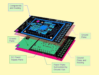
Another critical aspect of RF PCB design is the management of power distribution.
Ensuring a stable and clean power supply is vital for the proper functioning of RF circuits. The design software should be used to create robust power distribution networks, incorporating decoupling capacitors and power planes to minimize noise and voltage drops. Careful attention to grounding is also necessary, as poor grounding can lead to unwanted coupling and EMI. Implementing a solid ground plane and using vias to connect different layers can help maintain a low-impedance path to ground.
Thermal management is another consideration that should not be overlooked.
RF components can generate significant amounts of heat, which, if not properly managed, can degrade performance and reliability. The RF PCB design software can assist in simulating thermal behavior and identifying potential hotspots. Incorporating thermal vias, heat sinks, and appropriate spacing between components can aid in effective heat dissipation.
Finally, thorough validation and testing are essential to ensure that the design meets all performance criteria.
The RF PCB design software often includes simulation tools that allow designers to model the behavior of the circuit under various conditions. These simulations can identify potential issues before the physical prototype is built, saving time and resources. Once the design is finalized, it is prudent to conduct rigorous testing, including signal integrity analysis, EMI testing, and thermal analysis, to verify that the PCB performs as expected in real-world conditions.
In conclusion, leveraging RF PCB design software effectively requires a comprehensive understanding of RF principles, meticulous planning, and attention to detail throughout the design process. By adhering to these best practices, designers can create high-performance RF PCBs that meet the demanding requirements of modern applications.