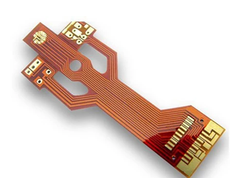
Rf pcb isolation
Importance Of Isolation In RF PCB isolation Design
In the realm of radio frequency (RF) printed circuit board (PCB) design, isolation plays a pivotal role in ensuring optimal performance and reliability. The importance of isolation in RF PCB design cannot be overstated, as it directly impacts signal integrity, electromagnetic compatibility (EMC), and overall system functionality. To fully appreciate the significance of isolation, it is essential to understand the various factors that contribute to its necessity and the methods employed to achieve it.
Firstly, signal integrity is a critical aspect of RF PCB design.
High-frequency signals are particularly susceptible to interference and crosstalk, which can degrade signal quality and lead to erroneous data transmission. Isolation helps mitigate these issues by preventing unwanted coupling between adjacent signal traces. By maintaining adequate spacing and employing ground planes, designers can minimize the risk of signal degradation and ensure that the transmitted signals remain clean and accurate.
Moreover, electromagnetic compatibility is another crucial consideration in RF PCB design.
RF circuits often operate in environments with numerous sources of electromagnetic interference (EMI), such as power supplies, digital circuits, and other RF components. Effective isolation techniques, such as shielding and the use of differential signaling, can significantly reduce the impact of EMI on the RF circuitry. This not only enhances the performance of the RF system but also ensures compliance with regulatory standards governing electromagnetic emissions.
In addition to signal integrity and EMC, isolation is vital for preventing unintended interactions between different sections of the PCB.
For instance, power supply noise can easily couple into sensitive RF circuits, leading to performance degradation.
By isolating the power supply and RF sections, designers can minimize the risk of noise coupling and maintain the integrity of the RF signals. This is particularly important in applications where high precision and low noise are paramount, such as in communication systems and instrumentation.
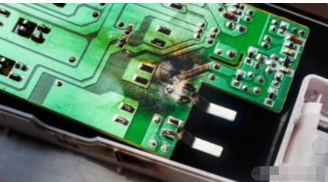
Furthermore, isolation is essential for thermal management in RF PCB design.
High-frequency components often generate significant amounts of heat, which can adversely affect the performance and longevity of the PCB. By isolating heat-generating components from sensitive RF circuitry, designers can prevent thermal-induced performance degradation and ensure the reliable operation of the RF system. This can be achieved through the use of thermal vias, heat sinks, and careful placement of components to facilitate efficient heat dissipation.
Transitioning to the methods employed to achieve isolation, designers have a variety of techniques at their disposal.
One common approach is the use of ground planes, which provide a low-impedance path for return currents and help shield sensitive RF traces from external interference. Additionally, the implementation of guard traces, which are grounded traces placed between signal lines, can further enhance isolation by reducing crosstalk.
Another effective technique is the use of differential signaling, where signals are transmitted as complementary pairs.
This approach not only improves signal integrity but also enhances immunity to common-mode noise, thereby improving overall isolation. Shielding, both at the component and PCB level, is also widely used to protect RF circuits from external EMI and to contain emissions within the PCB.
In conclusion, the importance of isolation in RF PCB design is multifaceted, encompassing signal integrity, electromagnetic compatibility, prevention of unintended interactions, and thermal management. By employing a combination of techniques such as ground planes, guard traces, differential signaling, and shielding, designers can achieve the necessary isolation to ensure optimal performance and reliability of RF systems. As RF technology continues to advance, the emphasis on effective isolation will remain a cornerstone of successful RF PCB design.
Techniques For Effective RF PCB Isolation
Effective RF PCB isolation is crucial in ensuring the optimal performance of radio frequency circuits. The primary goal of RF PCB isolation is to minimize interference and crosstalk between different circuit components, which can significantly degrade signal integrity and overall system performance. To achieve this, several techniques can be employed, each addressing specific aspects of isolation and contributing to a more robust design.
One fundamental technique for RF PCB isolation is the use of ground planes.
Ground planes serve as a reference point for all signals and provide a low-impedance path for return currents. By placing a continuous ground plane beneath the signal traces, designers can effectively shield the signals from external noise and reduce the potential for crosstalk. Additionally, ground planes help to maintain a consistent impedance, which is essential for preserving signal integrity in high-frequency circuits.
Another critical aspect of RF PCB isolation is the careful routing of signal traces.
Signal traces should be kept as short and direct as possible to minimize the potential for interference. When routing multiple signal traces, it is essential to maintain adequate spacing between them to prevent crosstalk. A general rule of thumb is to keep the spacing between traces at least three times the width of the trace itself. Furthermore, it is advisable to route high-frequency signals on a separate layer from low-frequency signals to reduce the risk of interference.
The use of via stitching is another effective technique for enhancing RF PCB isolation.
Via stitching involves placing multiple vias around the perimeter of a signal trace or ground plane to create a continuous conductive path. This helps to contain electromagnetic fields and prevent them from radiating into adjacent areas of the PCB. Via stitching is particularly useful in high-frequency applications where electromagnetic interference (EMI) can be a significant concern.
In addition to these techniques, the implementation of shielding can provide an extra layer of isolation for sensitive RF components.
Shielding can be achieved through the use of metal enclosures or cans that encase the RF circuitry. These shields act as a barrier, preventing external noise from entering the circuit and containing any emissions generated by the RF components. When designing shields, it is essential to ensure that they are properly grounded to the PCB to maximize their effectiveness.
Decoupling capacitors also play a vital role in RF PCB isolation.
These capacitors are placed between the power supply and ground to filter out high-frequency noise and provide a stable voltage supply to the RF components. By strategically placing decoupling capacitors close to the power pins of the RF devices, designers can significantly reduce the potential for noise coupling into the power supply lines.
Lastly, the use of differential signaling can enhance RF PCB isolation.
Differential signaling involves transmitting signals using two complementary traces, which helps to cancel out any noise that may be present. This technique is particularly effective in high-speed digital circuits, where maintaining signal integrity is paramount.
In conclusion, effective RF PCB isolation is achieved through a combination of techniques, including the use of ground planes, careful signal routing, via stitching, shielding, decoupling capacitors, and differential signaling. By employing these strategies, designers can minimize interference and crosstalk, ensuring the optimal performance of their RF circuits. Each technique addresses specific aspects of isolation, and when used in conjunction, they contribute to a more robust and reliable PCB design.
Common Mistakes In RF PCB Isolation And How To Avoid Them
In the realm of radio frequency (RF) printed circuit boards (PCBs), isolation is a critical factor that can significantly impact the performance and reliability of the final product. However, achieving optimal RF PCB isolation is fraught with challenges, and several common mistakes can undermine the effectiveness of the design. Understanding these pitfalls and learning how to avoid them is essential for engineers and designers striving for excellence in RF PCB development.
One prevalent mistake in RF PCB isolation is the improper placement of components.
Components that are too close to each other can lead to unwanted coupling and interference, which can degrade signal integrity. To avoid this, it is crucial to maintain adequate spacing between components, especially those that operate at different frequencies. Utilizing ground planes and shielding can further enhance isolation by providing a barrier against electromagnetic interference (EMI).
Another common error is the inadequate design of the ground plane.
A poorly designed ground plane can result in ground loops, which can introduce noise and reduce the overall performance of the RF PCB. To mitigate this issue, designers should ensure that the ground plane is continuous and free of gaps. Additionally, using multiple ground vias can help to minimize the inductance and improve the grounding effectiveness.
The use of inappropriate materials is also a frequent mistake in RF PCB isolation.
The choice of substrate material can have a significant impact on the dielectric constant and loss tangent, which in turn affect the signal propagation and isolation. Selecting materials with low dielectric constants and low loss tangents can help to minimize signal loss and improve isolation. Furthermore, it is essential to consider the thermal properties of the materials, as excessive heat can alter their electrical characteristics and compromise isolation.
Trace routing is another critical aspect where mistakes are often made.
Poorly routed traces can lead to crosstalk and signal degradation. To avoid this, designers should follow best practices for trace routing, such as maintaining consistent trace widths, using differential pairs for high-speed signals, and avoiding sharp bends. Additionally, keeping signal traces as short as possible and routing them away from noise sources can further enhance isolation.
The improper use of vias is another area where mistakes can occur.
Vias can introduce parasitic inductance and capacitance, which can affect signal integrity and isolation. To minimize these effects, it is advisable to use blind or buried vias instead of through-hole vias, as they can reduce the parasitic elements. Additionally, ensuring that vias are properly placed and connected to the ground plane can help to maintain isolation.
Finally, neglecting the importance of simulation and testing can lead to suboptimal RF PCB isolation.
Relying solely on theoretical designs without validating them through simulation and testing can result in unforeseen issues. Utilizing simulation tools to model the electromagnetic behavior of the PCB can help to identify potential problems and optimize the design. Moreover, conducting thorough testing, including signal integrity and EMI testing, can ensure that the PCB meets the desired isolation requirements.
In conclusion, achieving optimal RF PCB isolation requires careful consideration of various factors, including component placement, ground plane design, material selection, trace routing, via usage, and thorough simulation and testing. By avoiding common mistakes in these areas, designers can enhance the performance and reliability of their RF PCBs, ultimately leading to more successful and robust products.
Advanced Materials For Enhanced RF PCB Isolation
In the realm of radio frequency (RF) technology, the performance and reliability of printed circuit boards (PCBs) are paramount. One critical aspect that significantly influences these factors is RF PCB isolation. As the demand for higher frequencies and more compact designs continues to grow, the need for advanced materials to enhance RF PCB isolation becomes increasingly essential.
This article delves into the sophisticated materials that are being developed and utilized to achieve superior RF PCB isolation, thereby ensuring optimal performance and minimal interference.
To begin with, the primary objective of RF PCB isolation is to minimize electromagnetic interference (EMI) and crosstalk between different circuit components.
Traditional materials, such as FR-4, have been widely used in PCB manufacturing due to their cost-effectiveness and satisfactory performance at lower frequencies. However, as the frequency spectrum expands and the complexity of electronic devices increases, the limitations of conventional materials become apparent. Consequently, the industry is turning towards advanced materials that offer better dielectric properties, lower loss tangents, and improved thermal stability.
One such material that has gained prominence is polytetrafluoroethylene (PTFE), commonly known by the brand name Teflon.
PTFE-based laminates exhibit excellent dielectric properties, with a low dielectric constant and minimal loss tangent, making them ideal for high-frequency applications. Additionally, PTFE’s inherent thermal stability ensures that the material can withstand the heat generated during the operation of RF circuits, thereby maintaining consistent performance. The use of PTFE in RF PCB isolation not only enhances signal integrity but also reduces the risk of signal degradation over time.
Another advanced material that is making significant strides in RF PCB isolation is liquid crystal polymer (LCP).
LCPs are known for their exceptional electrical properties, including a low dielectric constant and low dissipation factor. These characteristics make LCPs highly suitable for high-frequency and high-speed applications. Moreover, LCPs offer excellent dimensional stability and low moisture absorption, which are critical for maintaining the integrity of RF signals in varying environmental conditions. The integration of LCPs into RF PCB designs ensures that the circuits remain isolated and free from unwanted interference, even in challenging operating environments.
Furthermore, ceramic-filled laminates are emerging as a viable option for enhancing RF PCB isolation.
These laminates combine the benefits of ceramics, such as high thermal conductivity and low dielectric loss, with the flexibility of traditional PCB materials. The result is a composite material that provides superior isolation and thermal management capabilities. Ceramic-filled laminates are particularly advantageous in applications where high power and high-frequency signals coexist, as they effectively dissipate heat and prevent signal distortion.
In addition to these materials, advancements in nanotechnology are paving the way for novel solutions in RF PCB isolation.
Nanocomposites, which incorporate nanoparticles into traditional PCB substrates, offer enhanced electrical and thermal properties. For instance, the inclusion of carbon nanotubes or graphene can significantly improve the dielectric constant and thermal conductivity of the substrate, leading to better isolation and heat dissipation. These nanocomposites represent the cutting edge of material science, promising to revolutionize the field of RF PCB design.
In conclusion, the quest for enhanced RF PCB isolation is driving the development and adoption of advanced materials. PTFE, LCPs, ceramic-filled laminates, and nanocomposites are at the forefront of this evolution, each offering unique benefits that address the challenges posed by high-frequency and high-power applications. As technology continues to advance, the integration of these materials into RF PCB designs will be crucial in achieving superior performance, reliability, and efficiency in electronic devices.