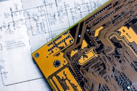
Rf pcb layout software
Key Features To Look For In RF PCB Layout Software
When selecting RF PCB layout software, it is crucial to consider several key features that can significantly impact the design process and the performance of the final product.
One of the primary aspects to evaluate is the software’s ability to handle high-frequency signals.
RF designs often operate at frequencies where even minor layout imperfections can lead to significant signal degradation. Therefore, the software must offer precise control over trace widths, spacing, and impedance matching to ensure signal integrity.
Another essential feature is the integration of electromagnetic (EM) simulation tools.
These tools allow designers to predict how electromagnetic fields will interact with the PCB layout, which is vital for identifying potential issues such as crosstalk, radiation, and signal loss. By incorporating EM simulation, designers can make informed decisions early in the design process, thereby reducing the need for costly and time-consuming revisions.
Additionally, the software should support advanced routing capabilities.
RF designs often require complex routing strategies to minimize signal interference and maintain performance. Features such as differential pair routing, controlled impedance routing, and the ability to manage via structures are indispensable. These capabilities enable designers to create layouts that meet stringent performance criteria while also adhering to manufacturing constraints.
Moreover, the software’s ability to handle multi-layer designs is another critical factor.
RF PCBs frequently utilize multiple layers to separate signal paths and power planes, which helps in reducing noise and improving overall performance. The software should provide robust tools for managing layer stack-ups, via placements, and inter-layer connections. This ensures that the design can be efficiently manufactured without compromising on performance.
Thermal management is another area where RF PCB layout software must excel.
High-frequency components often generate significant heat, which can affect both performance and reliability. The software should offer thermal analysis tools to help designers identify hotspots and optimize the layout for better heat dissipation. This can include features like thermal vias, heat sinks, and proper placement of components to ensure efficient thermal management.
Furthermore, the software should facilitate seamless collaboration among team members.
Modern RF PCB designs often involve multiple engineers working on different aspects of the project. Features such as version control, real-time collaboration, and design review tools can greatly enhance productivity and reduce the likelihood of errors. These collaborative tools ensure that all team members are on the same page, thereby streamlining the design process.
In addition to these technical features, ease of use is also an important consideration.
The software should have an intuitive user interface that allows designers to quickly learn and utilize its features. Comprehensive documentation, tutorials, and customer support can further enhance the user experience, making it easier for designers to focus on creating high-quality RF PCB layouts.
Lastly, compatibility with other design tools and file formats is essential.
RF PCB layout software should be able to import and export files in various formats to ensure smooth integration with other design and simulation tools. This interoperability is crucial for maintaining a cohesive design workflow and ensuring that all aspects of the project are aligned.
In conclusion, selecting the right RF PCB layout software involves evaluating a range of features that collectively contribute to the efficiency and effectiveness of the design process. From high-frequency signal handling and EM simulation to advanced routing capabilities and thermal management, each feature plays a vital role in ensuring the success of RF PCB designs. By carefully considering these aspects, designers can choose software that not only meets their technical requirements but also enhances their overall productivity and collaboration.
Best Practices For Designing RF PCBs Using Layout Software
Designing RF PCBs (Radio Frequency Printed Circuit Boards) using layout software requires a meticulous approach to ensure optimal performance and reliability. The complexity of RF circuits necessitates adherence to best practices that address signal integrity, electromagnetic interference (EMI), and thermal management. By following these guidelines, designers can leverage layout software to create efficient and effective RF PCBs.
To begin with, understanding the importance of component placement is crucial.
In RF PCB design, the placement of components significantly impacts signal integrity and overall performance. It is advisable to position high-frequency components, such as oscillators and amplifiers, as close to each other as possible to minimize signal path lengths. This reduces the potential for signal degradation and EMI. Additionally, placing sensitive components away from noisy power supplies and digital circuits can further enhance performance.
Transitioning to the topic of trace routing, it is essential to maintain controlled impedance throughout the PCB.
Controlled impedance ensures that the signal transmission remains consistent, reducing reflections and signal loss. Utilizing layout software, designers can define trace widths and spacing to achieve the desired impedance. Moreover, employing differential pairs for high-speed signals can help mitigate noise and crosstalk, thereby improving signal integrity.
Another critical aspect of RF PCB design is the use of ground planes.
Ground planes provide a low-impedance path for return currents, which is vital for maintaining signal integrity and reducing EMI. It is recommended to use a continuous ground plane on at least one layer of the PCB. This practice not only enhances signal performance but also simplifies the design process by providing a common reference point for all components. Furthermore, stitching vias can be employed to connect multiple ground planes, ensuring a robust grounding system.
Thermal management is another key consideration in RF PCB design.
High-frequency components often generate significant heat, which can affect performance and reliability if not properly managed. Layout software can assist in designing thermal vias and heat sinks to dissipate heat effectively. Additionally, placing thermal pads under heat-generating components and ensuring adequate airflow can further enhance thermal performance.
Incorporating proper shielding techniques is also vital in RF PCB design.
Shielding helps to isolate sensitive components from external noise sources and prevents EMI from affecting other parts of the circuit. Layout software can facilitate the design of shielding enclosures and the placement of ground traces around critical areas. By implementing these techniques, designers can achieve a higher level of signal integrity and overall performance.
Moreover, the selection of appropriate materials plays a significant role in RF PCB design.
High-frequency signals are more susceptible to losses and dispersion, making the choice of substrate material critical. Materials with low dielectric constant and low loss tangent are preferred for RF applications. Layout software can assist in simulating the performance of different materials, enabling designers to make informed decisions.
Finally, thorough testing and validation are indispensable in RF PCB design.
After completing the layout, it is essential to perform simulations and signal integrity analysis using the layout software. These tools can identify potential issues such as impedance mismatches, signal reflections, and EMI. By addressing these issues early in the design process, designers can avoid costly revisions and ensure the final product meets performance specifications.
In conclusion, designing RF PCBs using layout software involves a comprehensive approach that encompasses component placement, trace routing, grounding, thermal management, shielding, material selection, and thorough testing. By adhering to these best practices, designers can create RF PCBs that deliver optimal performance and reliability, ultimately contributing to the success of their projects.
Comparing Popular RF PCB Layout Software Tools
When it comes to designing radio frequency (RF) printed circuit boards (PCBs), the choice of layout software can significantly impact the efficiency and success of the project. Several RF PCB layout software tools are available, each offering unique features and capabilities tailored to meet the specific needs of engineers and designers. In this article, we will compare some of the most popular RF PCB layout software tools, examining their strengths and weaknesses to help you make an informed decision.
One of the most widely recognized RF PCB layout software tools is Altium Designer.
Known for its comprehensive suite of features, Altium Designer provides a robust platform for designing complex RF circuits. It offers advanced simulation capabilities, allowing designers to model and analyze RF behavior before committing to physical prototypes. Additionally, Altium Designer’s user-friendly interface and extensive library of components make it a preferred choice for many professionals. However, its high cost can be a barrier for smaller firms or individual designers.
Another prominent tool in the RF PCB layout domain is Cadence Allegro.
Cadence Allegro is renowned for its high-performance design environment, which supports intricate RF designs with precision. The software excels in handling large-scale projects, offering powerful routing and signal integrity analysis tools. Furthermore, Cadence Allegro’s integration with other Cadence products facilitates a seamless workflow for those already using the Cadence ecosystem. Despite its advanced capabilities, the steep learning curve associated with Cadence Allegro may deter beginners or those unfamiliar with its interface.
Mentor Graphics’ PADS Professional is another noteworthy contender in the RF PCB layout software market.
PADS Professional combines ease of use with advanced functionality, making it suitable for both novice and experienced designers. The software’s RF design capabilities are bolstered by its robust simulation tools, which help in predicting and mitigating potential issues early in the design process. Moreover, PADS Professional’s affordability compared to other high-end tools makes it an attractive option for small to medium-sized enterprises. Nevertheless, some users may find its feature set less comprehensive than that of more expensive alternatives.
Keysight Technologies’ Advanced Design System (ADS) is specifically tailored for RF and microwave design, making it a specialized tool in this field.
ADS offers unparalleled simulation accuracy, thanks to its extensive library of RF models and components. The software’s ability to co-simulate with other Keysight tools enhances its versatility, providing a holistic approach to RF design. However, the specialized nature of ADS means it may not be as versatile for non-RF applications, and its cost can be prohibitive for some users.
Finally, Autodesk’s Eagle is a popular choice among hobbyists and small businesses due to its affordability and ease of use.
While not as feature-rich as some of the more expensive tools, Eagle offers sufficient capabilities for basic to intermediate RF PCB designs. Its integration with Autodesk’s Fusion 360 also provides a pathway for mechanical and electronic co-design, which can be beneficial for certain projects. However, for highly complex RF designs, Eagle may fall short in terms of advanced simulation and analysis features.
In conclusion, the choice of RF PCB layout software depends largely on the specific needs and constraints of the designer or organization. Altium Designer and Cadence Allegro offer comprehensive, high-end solutions suitable for complex projects, albeit at a higher cost and with steeper learning curves. PADS Professional strikes a balance between functionality and affordability, making it a viable option for many. ADS stands out for its specialized RF capabilities, while Eagle provides a cost-effective solution for simpler designs. By carefully considering the features, costs, and learning requirements of each tool, designers can select the software that best aligns with their project goals and resources.
How RF PCB Layout Software Enhances Signal Integrity
In the realm of modern electronics, maintaining signal integrity is paramount, particularly in radio frequency (RF) applications where even minor disruptions can lead to significant performance degradation. RF PCB layout software plays a crucial role in ensuring that signal integrity is preserved throughout the design and manufacturing process. By leveraging advanced algorithms and sophisticated design tools, these software solutions enable engineers to create layouts that minimize interference, reduce signal loss, and enhance overall system performance.
One of the primary ways RF PCB layout software enhances signal integrity is through meticulous impedance control.
Impedance mismatches can lead to signal reflections, which in turn cause signal degradation and loss. RF PCB layout software allows designers to precisely control the impedance of transmission lines by adjusting trace widths, spacing, and the dielectric properties of the substrate. This level of control ensures that the impedance remains consistent throughout the circuit, thereby minimizing reflections and maintaining signal integrity.
Moreover, RF PCB layout software provides powerful simulation tools that enable designers to predict and mitigate potential issues before they manifest in the physical prototype.
Electromagnetic simulation, for instance, allows engineers to visualize how signals will propagate through the PCB and identify areas where interference or crosstalk may occur. By addressing these issues in the design phase, engineers can make informed decisions about trace routing, grounding, and shielding, ultimately leading to a more robust and reliable PCB.
In addition to simulation, RF PCB layout software often includes design rule checks (DRCs) that automatically verify the layout against a set of predefined criteria.
These checks can identify potential problems such as insufficient spacing between traces, inadequate grounding, or violations of manufacturing constraints. By catching these issues early in the design process, DRCs help ensure that the final PCB will perform as intended, without the need for costly and time-consuming revisions.
Another critical aspect of RF PCB layout software is its ability to facilitate effective grounding and shielding strategies.
Proper grounding is essential for minimizing noise and preventing signal degradation, while shielding helps protect sensitive components from external electromagnetic interference (EMI). RF PCB layout software provides tools for designing ground planes, stitching vias, and implementing shielding enclosures, all of which contribute to maintaining signal integrity. By optimizing these elements, designers can create PCBs that are less susceptible to noise and interference, thereby enhancing overall performance.
Furthermore, RF PCB layout software often includes features for thermal management, which is another important factor in maintaining signal integrity.
Excessive heat can cause components to drift out of their specified operating ranges, leading to signal distortion and potential failure. By incorporating thermal analysis tools, RF PCB layout software enables designers to identify hotspots and implement cooling solutions such as heat sinks, thermal vias, and optimized trace layouts. Effective thermal management ensures that the PCB operates within safe temperature limits, thereby preserving signal integrity over the long term.
In conclusion, RF PCB layout software is an indispensable tool for engineers seeking to enhance signal integrity in their designs. Through precise impedance control, advanced simulation capabilities, rigorous design rule checks, effective grounding and shielding strategies, and robust thermal management, these software solutions provide a comprehensive approach to maintaining signal integrity. By leveraging the capabilities of RF PCB layout software, designers can create high-performance PCBs that meet the demanding requirements of modern RF applications, ensuring reliable and efficient operation in a wide range of environments.


