Rf pcb prototype
Designing Efficient RF PCB Prototypes: Best Practices
Designing efficient RF PCB prototypes is a critical task that demands meticulous attention to detail and a deep understanding of both the theoretical and practical aspects of radio frequency (RF) engineering. The process begins with a comprehensive understanding of the specific requirements and constraints of the project. This includes the frequency range, power levels, and the intended application of the RF circuit. By clearly defining these parameters, designers can make informed decisions about the materials, layout, and components that will be used in the prototype.
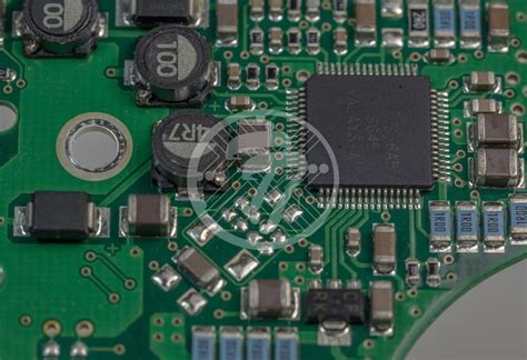
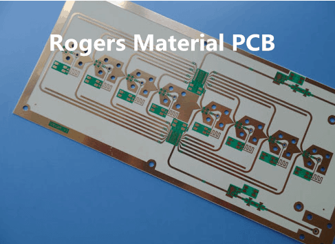
One of the fundamental considerations in RF PCB design is the choice of substrate material.
The dielectric constant and loss tangent of the substrate significantly impact the performance of the RF circuit. Materials such as Rogers, Teflon, and FR4 are commonly used, each offering different advantages and trade-offs. For instance, Rogers materials are known for their low loss and stable dielectric properties, making them suitable for high-frequency applications. However, they are also more expensive compared to FR4, which is widely used for its cost-effectiveness but may not perform as well at higher frequencies.
Transitioning from material selection to layout design, it is essential to minimize signal loss and interference.
This can be achieved by carefully planning the placement of components and routing of traces. The use of ground planes is a common practice to provide a low-impedance path for return currents and to shield sensitive components from electromagnetic interference (EMI). Additionally, maintaining consistent trace widths and spacing is crucial to ensure impedance matching, which is vital for minimizing signal reflections and losses.
Another important aspect of RF PCB design is the management of power distribution.
Ensuring a stable and clean power supply is paramount, as noise and fluctuations can severely degrade the performance of RF circuits. Decoupling capacitors should be strategically placed near power pins of active components to filter out high-frequency noise. Furthermore, the use of power planes can help in distributing power evenly across the board, reducing voltage drops and improving overall performance.
Thermal management is also a key consideration in RF PCB design.
High-power RF components can generate significant amounts of heat, which, if not properly managed, can lead to performance degradation or even failure. Effective thermal management strategies include the use of thermal vias, heat sinks, and careful placement of heat-generating components to ensure efficient heat dissipation.
In addition to these technical considerations, it is important to conduct thorough testing and validation of the RF PCB prototype.
This involves using specialized equipment such as network analyzers, spectrum analyzers, and oscilloscopes to measure parameters like return loss, insertion loss, and signal integrity. By rigorously testing the prototype, designers can identify and address any issues before moving on to mass production.
Finally, collaboration and communication among team members are essential throughout the design process.
RF PCB design often involves multiple disciplines, including electrical engineering, mechanical engineering, and materials science. By fostering a collaborative environment, teams can leverage diverse expertise to optimize the design and ensure that all aspects of the project are considered.
In conclusion, designing efficient RF PCB prototypes requires a holistic approach that encompasses material selection, layout design, power distribution, thermal management, and thorough testing. By adhering to best practices and maintaining a collaborative mindset, designers can create high-performance RF circuits that meet the stringent demands of modern applications.
Common Challenges in RF PCB Prototyping and How to Overcome Them
RF PCB prototyping is a critical phase in the development of radio frequency circuits, which are integral to a wide range of applications, from telecommunications to medical devices. However, this process is fraught with challenges that can impede progress and affect the performance of the final product. Understanding these common challenges and knowing how to overcome them is essential for engineers and designers working in this field.
One of the primary challenges in RF PCB prototyping is signal integrity.
High-frequency signals are particularly susceptible to interference and loss, which can degrade performance. To mitigate this, careful attention must be paid to the layout of the PCB. Ensuring that signal paths are as short as possible and avoiding sharp bends can help maintain signal integrity. Additionally, using high-quality materials with low dielectric loss can reduce signal attenuation.
Another significant challenge is impedance matching.
Mismatched impedance can lead to signal reflections, which can cause interference and reduce the efficiency of the circuit. To address this, designers must carefully calculate and match the impedance of transmission lines and components. Utilizing tools such as Smith charts and network analyzers can aid in achieving precise impedance matching.
Thermal management is also a critical concern in RF PCB prototyping.
High-frequency circuits often generate significant amounts of heat, which can affect performance and reliability. Effective thermal management strategies, such as the use of thermal vias, heat sinks, and proper component placement, are essential to dissipate heat efficiently. Additionally, selecting materials with good thermal conductivity can further enhance thermal management.
Electromagnetic interference (EMI) is another common issue in RF PCB prototyping.
EMI can originate from various sources, including other electronic devices and even the PCB itself. To minimize EMI, designers should implement proper shielding techniques and maintain adequate spacing between components. Ground planes and decoupling capacitors can also help reduce EMI by providing a stable reference point and filtering out noise.
Component selection is a crucial aspect that can pose challenges in RF PCB prototyping.
The performance of RF circuits is highly dependent on the quality and specifications of the components used. Therefore, selecting components with appropriate frequency ratings, tolerances, and thermal characteristics is vital. Collaborating with component manufacturers and suppliers can provide valuable insights and ensure that the right components are chosen for the design.
Moreover, the manufacturing process itself can introduce challenges.
Variations in the fabrication process, such as etching precision and layer alignment, can affect the performance of the RF PCB. Working closely with experienced PCB manufacturers and specifying tight tolerances can help mitigate these issues. Additionally, conducting thorough testing and validation of prototypes can identify and address any manufacturing-related problems early in the development process.
In conclusion, RF PCB prototyping presents a range of challenges that require careful consideration and expertise to overcome. By focusing on signal integrity, impedance matching, thermal management, EMI reduction, component selection, and manufacturing precision, designers can enhance the performance and reliability of their RF circuits. Leveraging advanced tools and collaborating with experienced partners can further streamline the prototyping process and lead to successful outcomes. As technology continues to evolve, staying abreast of the latest developments and best practices in RF PCB design will be essential for engineers and designers to navigate these challenges effectively.
Materials and Techniques for High-Performance RF PCB Prototypes
In the realm of high-frequency electronics, the development of Radio Frequency (RF) Printed Circuit Board (PCB) prototypes necessitates meticulous attention to materials and techniques to ensure optimal performance. The selection of appropriate materials and the application of advanced fabrication techniques are paramount in achieving the desired electrical characteristics and reliability of RF PCBs. This article delves into the critical aspects of materials and techniques that are instrumental in the creation of high-performance RF PCB prototypes.
To begin with, the choice of substrate material is a fundamental consideration in RF PCB design.
Unlike standard PCBs, which often utilize FR-4 material, RF PCBs require substrates with superior dielectric properties to minimize signal loss and maintain signal integrity at high frequencies. Materials such as Rogers RT/duroid, Taconic, and Arlon are frequently employed due to their low dielectric constant (Dk) and low dissipation factor (Df). These materials offer excellent thermal stability and consistent electrical performance, which are crucial for RF applications. The low Dk ensures minimal signal delay, while the low Df reduces signal attenuation, thereby enhancing the overall performance of the RF PCB.
In addition to substrate selection, the copper cladding used in RF PCBs plays a significant role in determining the board’s performance.
High-frequency signals are particularly susceptible to losses due to skin effect, where the signal tends to travel on the surface of the conductor. Therefore, the use of high-purity, smooth copper foil is essential to minimize these losses. Electrodeposited (ED) copper and rolled annealed (RA) copper are commonly used, with RA copper being preferred for its smoother surface and better performance at high frequencies.
Furthermore, the design and layout of RF PCBs require careful consideration to mitigate issues such as crosstalk, electromagnetic interference (EMI), and signal reflection. Techniques such as controlled impedance routing, proper grounding, and the use of microstrip or stripline configurations are employed to ensure signal integrity. Controlled impedance routing involves maintaining a consistent impedance along the signal path, which is critical for high-frequency signals. Proper grounding techniques, including the use of ground planes and via stitching, help in reducing EMI and providing a stable reference for signal return paths. Microstrip and stripline configurations are used to control the electromagnetic fields around the signal traces, thereby minimizing signal loss and crosstalk.
Moreover, the fabrication process of RF PCBs demands precision and adherence to stringent tolerances.
Advanced manufacturing techniques such as laser drilling, precision etching, and sequential lamination are utilized to achieve the required accuracy. Laser drilling is employed for creating microvias, which are essential for high-density interconnects and reducing signal path lengths. Precision etching ensures that the trace widths and spacing are maintained within tight tolerances, which is crucial for controlled impedance. Sequential lamination allows for the construction of multilayer PCBs with complex layer stacks, providing the necessary interconnections and shielding for high-frequency signals.
In conclusion, the development of high-performance RF PCB prototypes hinges on the judicious selection of materials and the application of advanced fabrication techniques. The use of specialized substrate materials, high-quality copper cladding, and meticulous design practices are essential in achieving the desired electrical performance and reliability. As the demand for high-frequency applications continues to grow, the importance of these considerations in RF PCB design and fabrication cannot be overstated. By adhering to these principles, engineers can ensure the successful realization of RF PCB prototypes that meet the stringent requirements of modern high-frequency electronics.
Innovative Tools and Software for RF PCB Prototype Development
The development of RF PCB prototypes has seen significant advancements in recent years, driven by innovative tools and software that streamline the design and testing processes. These advancements are crucial for engineers and designers who aim to create high-performance RF circuits with precision and efficiency. The integration of sophisticated software tools with advanced hardware capabilities has revolutionized the way RF PCB prototypes are developed, ensuring that the final products meet stringent performance criteria.
One of the most notable innovations in this field is the advent of computer-aided design (CAD) software specifically tailored for RF PCB design.
These software solutions offer a range of features that facilitate the intricate process of designing RF circuits. For instance, they provide comprehensive libraries of components, which include detailed specifications and models that can be easily integrated into the design. This not only saves time but also ensures that the components used are compatible with the desired performance parameters. Additionally, these CAD tools often come with simulation capabilities that allow designers to test their circuits virtually before moving on to physical prototyping. This step is crucial as it helps identify potential issues early in the design process, thereby reducing the risk of costly errors.
Moreover, the use of electromagnetic (EM) simulation software has become increasingly prevalent in RF PCB prototype development.
EM simulation tools enable designers to analyze the electromagnetic behavior of their circuits in a virtual environment. This is particularly important for RF designs, where signal integrity and electromagnetic interference (EMI) are critical concerns. By simulating the electromagnetic fields and their interactions within the circuit, designers can optimize the layout to minimize interference and ensure robust performance. This level of analysis was previously unattainable with traditional design methods, highlighting the transformative impact of these innovative tools.
In addition to software advancements, hardware tools have also evolved to support the development of RF PCB prototypes.
Modern prototyping equipment, such as precision milling machines and laser cutters, allows for the rapid and accurate fabrication of PCB prototypes. These machines can produce intricate designs with high precision, which is essential for RF circuits that often require fine geometries and tight tolerances. Furthermore, advancements in materials science have led to the development of specialized substrates and laminates that offer superior performance for RF applications. These materials exhibit low dielectric losses and high thermal stability, which are critical for maintaining signal integrity and reliability in RF circuits.
The integration of these innovative tools and software has also facilitated a more collaborative approach to RF PCB prototype development.
Cloud-based platforms and collaborative design environments enable teams to work together seamlessly, regardless of their geographical locations. This fosters a more efficient workflow, as team members can share designs, simulations, and test results in real-time, leading to faster iterations and improved outcomes. Additionally, these platforms often include version control and project management features, which help streamline the development process and ensure that all team members are aligned.
In conclusion, the development of RF PCB prototypes has been significantly enhanced by the advent of innovative tools and software. The combination of advanced CAD and EM simulation software, precision prototyping equipment, and collaborative platforms has transformed the way RF circuits are designed and tested. These advancements not only improve the efficiency and accuracy of the development process but also ensure that the final products meet the high-performance standards required for modern RF applications. As technology continues to evolve, it is likely that we will see even more sophisticated tools and methods emerge, further pushing the boundaries of what is possible in RF PCB prototype development.