Rf pcb routing guidelines
Best Practices For RF PCB Routing
When designing RF (Radio Frequency) printed circuit boards (PCBs), adhering to best practices for routing is crucial to ensure optimal performance and signal integrity. The complexity of RF signals, which operate at high frequencies, necessitates meticulous attention to detail in the PCB layout process.
To begin with, one of the fundamental principles in RF PCB routing is to minimize the length of signal traces.
Shorter traces reduce the potential for signal loss and minimize the risk of interference. This is particularly important because longer traces can act as antennas, inadvertently radiating or picking up unwanted signals.
In addition to keeping traces short, maintaining consistent trace impedance is essential.
Impedance mismatches can lead to signal reflections, which degrade signal quality. To achieve consistent impedance, designers often use controlled impedance traces, which involve carefully selecting the trace width and the distance between the trace and the reference plane. This practice ensures that the signal travels smoothly without encountering impedance discontinuities.
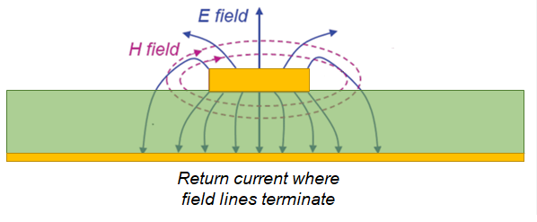
Another critical aspect of RF PCB routing is the use of ground planes.
Ground planes provide a low-impedance return path for RF signals, which helps to reduce noise and improve signal integrity. It is advisable to have a continuous ground plane beneath the RF traces to minimize the loop area and, consequently, the inductance. This approach also aids in shielding the RF signals from external electromagnetic interference (EMI).
Furthermore, the placement of components plays a significant role in RF PCB design.
Components should be strategically placed to minimize the length of RF signal paths and to avoid crossing sensitive analog or digital traces. Placing components in close proximity to each other can help reduce parasitic inductance and capacitance, which can adversely affect the performance of the RF circuit.
Transitioning to the topic of vias, it is important to note that vias can introduce inductance and capacitance, which can impact the performance of RF signals.
Therefore, the use of vias should be minimized, and when necessary, they should be placed carefully. For instance, using multiple vias in parallel can help reduce the inductance and provide a more robust connection between layers.
Moreover, the choice of materials for the PCB substrate is another critical consideration.
High-frequency signals are more susceptible to losses in the dielectric material of the PCB. Therefore, selecting a low-loss dielectric material, such as Rogers or Teflon, can significantly improve the performance of RF circuits. These materials have lower dielectric constants and loss tangents, which help maintain signal integrity at high frequencies.
Thermal management is also an important factor in RF PCB design.
High-frequency components can generate significant amounts of heat, which can affect their performance and reliability. Implementing proper thermal management techniques, such as using thermal vias and heat sinks, can help dissipate heat effectively and maintain the stability of the RF circuit.
Lastly, simulation and testing are indispensable steps in the RF PCB design process.
Using simulation tools to model the PCB layout can help identify potential issues and optimize the design before fabrication. Once the PCB is fabricated, thorough testing should be conducted to verify that the design meets the required performance specifications.
In conclusion, following best practices for RF PCB routing is essential to achieve high-performance and reliable RF circuits. By minimizing trace lengths, maintaining consistent impedance, using ground planes, strategically placing components, carefully managing vias, selecting appropriate materials, and implementing effective thermal management, designers can ensure the integrity and efficiency of their RF PCB designs.

Minimizing Signal Loss In RF PCB Design
Minimizing signal loss in RF PCB design is a critical aspect that demands meticulous attention to detail and a comprehensive understanding of various influencing factors. Signal loss, often referred to as attenuation, can significantly degrade the performance of RF circuits, leading to inefficiencies and potential failures in communication systems. To mitigate these issues, several guidelines must be adhered to during the design and routing of RF PCBs.
Firstly, the choice of materials plays a pivotal role in minimizing signal loss.
High-frequency signals are particularly susceptible to losses caused by the dielectric properties of the PCB substrate. Therefore, selecting a substrate with a low dielectric constant (Dk) and low dissipation factor (Df) is essential. Materials such as Rogers or Teflon are often preferred over standard FR-4 due to their superior high-frequency performance. These materials help in reducing dielectric losses, thereby preserving signal integrity.
In addition to material selection, the physical layout of the PCB is equally important.
The length of the transmission lines should be minimized to reduce resistive losses. Longer traces introduce higher resistance, which in turn increases signal attenuation. Moreover, maintaining consistent trace widths is crucial. Variations in trace width can cause impedance mismatches, leading to reflections and further signal loss. Utilizing controlled impedance traces ensures that the signal travels with minimal distortion.
Another critical factor is the use of proper grounding techniques.
A solid and continuous ground plane is indispensable in RF PCB design. It provides a return path for the signal and helps in minimizing electromagnetic interference (EMI). Ensuring that the ground plane is as close as possible to the signal traces reduces the loop area, thereby decreasing inductive losses. Additionally, via stitching can be employed to connect multiple ground planes, further enhancing the grounding effectiveness.
The placement of components also significantly impacts signal loss.
Components should be strategically placed to minimize the length of interconnecting traces. For instance, placing RF components such as amplifiers, mixers, and filters close to each other reduces the trace length and, consequently, the associated losses. Furthermore, avoiding sharp bends in traces is advisable. Sharp bends can cause impedance discontinuities, leading to signal reflections and increased loss. Instead, using gradual curves or mitered bends helps maintain consistent impedance.
Shielding is another technique that can be employed to minimize signal loss.
RF signals are prone to external interference, which can introduce noise and degrade signal quality. Implementing shielding techniques, such as using metal enclosures or ground planes, can effectively isolate the RF signals from external noise sources. This isolation helps in preserving the signal integrity and reducing losses.
Moreover, the use of proper termination techniques is essential in RF PCB design.
Unmatched terminations can cause reflections, leading to signal loss and potential damage to components. Ensuring that all transmission lines are properly terminated with their characteristic impedance helps in minimizing reflections and maintaining signal integrity.
In conclusion, minimizing signal loss in RF PCB design requires a holistic approach that encompasses material selection, physical layout, grounding techniques, component placement, shielding, and proper termination. By adhering to these guidelines, designers can significantly enhance the performance and reliability of RF circuits. The meticulous implementation of these strategies ensures that the high-frequency signals are transmitted with minimal attenuation, thereby optimizing the overall functionality of the RF system.
Importance Of Ground Planes In RF PCB Routing
In the realm of RF PCB routing, the importance of ground planes cannot be overstated. Ground planes serve as a fundamental component in ensuring the optimal performance of RF circuits, providing a stable reference point for signals and minimizing electromagnetic interference (EMI). As RF signals are highly susceptible to noise and interference, the implementation of ground planes becomes crucial in maintaining signal integrity and achieving reliable circuit functionality.
To begin with, ground planes offer a low-impedance path to ground, which is essential for the proper functioning of RF circuits.
By providing a continuous conductive surface, ground planes help in reducing the inductance and resistance of the return path, thereby minimizing voltage drops and ensuring a stable reference potential. This stability is particularly important in high-frequency applications, where even minor variations in the ground potential can lead to significant signal degradation.
Moreover, ground planes play a pivotal role in controlling EMI.
In RF circuits, signals are transmitted at high frequencies, which can lead to the generation of unwanted electromagnetic radiation. Ground planes act as shields, absorbing and redirecting this radiation away from sensitive components and traces. This shielding effect helps in preventing cross-talk between adjacent signal lines and reduces the risk of interference from external sources. Consequently, the overall electromagnetic compatibility (EMC) of the PCB is enhanced, ensuring that the circuit operates within the desired parameters without causing or being affected by EMI.
In addition to EMI control, ground planes also contribute to the reduction of signal reflections and impedance mismatches.
When RF signals travel through a PCB, they encounter various discontinuities, such as vias, connectors, and component pads. These discontinuities can cause signal reflections, leading to signal loss and distortion. Ground planes help in mitigating these reflections by providing a continuous reference plane, which ensures that the characteristic impedance of the transmission lines remains consistent. This impedance matching is critical for maintaining signal integrity and minimizing losses, especially in high-frequency applications.
Furthermore, the use of ground planes facilitates efficient heat dissipation.
RF circuits often generate significant amounts of heat, which can adversely affect the performance and reliability of the components. Ground planes, with their large surface area and good thermal conductivity, help in spreading and dissipating this heat more effectively. This thermal management is essential for preventing overheating and ensuring the longevity of the PCB and its components.
It is also worth noting that the placement and design of ground planes require careful consideration.
Ideally, ground planes should be placed on a dedicated layer, separate from signal and power layers, to minimize interference and ensure a clear return path for signals. Additionally, maintaining a continuous and unbroken ground plane is crucial, as any gaps or discontinuities can lead to increased impedance and signal degradation. Proper via stitching and grounding techniques should be employed to connect different ground planes and ensure a uniform potential across the PCB.
In conclusion, ground planes are indispensable in RF PCB routing, providing a stable reference point, controlling EMI, reducing signal reflections, and facilitating heat dissipation. Their implementation requires meticulous planning and design to ensure optimal performance and reliability of RF circuits. By adhering to these guidelines, designers can achieve superior signal integrity and electromagnetic compatibility, ultimately leading to more efficient and robust RF systems.
Techniques For Reducing EMI In RF PCB Layouts
Electromagnetic interference (EMI) is a critical concern in the design of radio frequency (RF) printed circuit boards (PCBs). Effective techniques for reducing EMI are essential to ensure the optimal performance and reliability of RF circuits. One fundamental approach to mitigating EMI is to carefully manage the layout of the PCB. This involves strategic placement of components, meticulous routing of traces, and the implementation of grounding and shielding techniques.
To begin with, the placement of components plays a pivotal role in minimizing EMI.
It is advisable to position high-frequency components as close to each other as possible. This reduces the length of the signal paths, thereby minimizing the potential for radiated emissions. Additionally, sensitive analog components should be kept away from noisy digital circuits to prevent interference. By segregating analog and digital sections of the PCB, designers can create a more controlled environment for each type of signal.
Transitioning to the routing of traces, it is crucial to keep signal traces as short and direct as possible.
Long traces can act as antennas, radiating unwanted electromagnetic waves. To further reduce EMI, differential pairs should be routed together with a consistent spacing to maintain their characteristic impedance. This helps to cancel out common-mode noise. Moreover, avoiding sharp bends in traces is important, as these can cause reflections and increase EMI. Instead, using smooth, gradual curves can help maintain signal integrity.
Grounding is another essential technique for reducing EMI in RF PCB layouts.
A solid ground plane provides a low-impedance path for return currents, which helps to minimize noise. It is beneficial to use a continuous ground plane on one layer of the PCB, ensuring that it is not fragmented by signal traces. Stitching vias can be employed to connect different ground planes, further enhancing the grounding effectiveness. Additionally, placing decoupling capacitors close to power pins of active components can help to filter out high-frequency noise, thereby reducing EMI.
Shielding is also a valuable method for controlling EMI.
Metal shields can be placed over sensitive components or entire sections of the PCB to block external electromagnetic fields. This is particularly useful in environments with high levels of ambient EMI. However, it is important to ensure that the shields are properly grounded to prevent them from becoming sources of interference themselves.
Another technique involves the use of controlled impedance traces.
By designing traces with specific impedance values, signal reflections can be minimized, which in turn reduces EMI. This requires careful consideration of the trace width, spacing, and the dielectric properties of the PCB material. Controlled impedance is especially important for high-speed signals, where even small impedance mismatches can lead to significant EMI issues.
In conclusion, reducing EMI in RF PCB layouts requires a comprehensive approach that encompasses component placement, trace routing, grounding, shielding, and controlled impedance. By meticulously applying these techniques, designers can create RF circuits that are less susceptible to interference, thereby enhancing their performance and reliability. The integration of these strategies into the design process is essential for achieving optimal results in RF PCB layouts.


