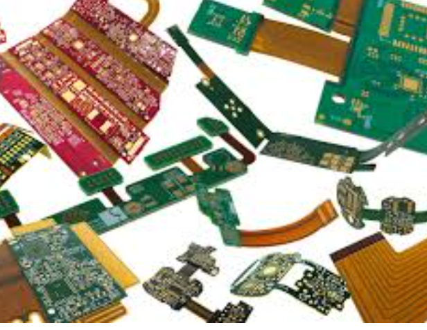
Rigid-flex pcb design guide
Benefits Of Rigid-Flex PCB Design In Modern Electronics
Rigid-flex PCB design has emerged as a pivotal innovation in the realm of modern electronics, offering a multitude of benefits that cater to the evolving demands of contemporary technology. This hybrid approach, which combines the advantages of both rigid and flexible circuit boards, has revolutionized the way electronic devices are designed and manufactured.
One of the foremost benefits of rigid-flex PCB design is its ability to enhance the reliability and durability of electronic devices.
By integrating flexible circuits with rigid boards, the design minimizes the number of interconnects and solder joints, which are often points of failure in traditional PCB assemblies. This reduction in potential failure points translates to increased longevity and robustness, making rigid-flex PCBs particularly suitable for applications in harsh environments or where mechanical stress is a concern.
In addition to improved reliability, rigid-flex PCB design offers significant space and weight savings.
The flexible sections of the PCB can be bent and folded to fit into compact spaces, allowing for more efficient use of available real estate within a device. This is especially advantageous in the design of portable and wearable electronics, where size and weight are critical factors. The ability to create three-dimensional configurations with rigid-flex PCBs also enables more innovative and compact product designs, pushing the boundaries of what is possible in modern electronics.
Another notable benefit of rigid-flex PCB design is its contribution to enhanced signal integrity and performance.
The seamless integration of rigid and flexible sections allows for shorter and more direct signal paths, reducing the risk of signal loss and electromagnetic interference. This is particularly important in high-frequency applications, where maintaining signal integrity is crucial for optimal performance. Furthermore, the inherent flexibility of the design can help absorb and mitigate mechanical vibrations, further protecting the integrity of the signals.
The manufacturing process of rigid-flex PCBs also offers advantages in terms of assembly and testing.
The integration of multiple rigid and flexible layers into a single board reduces the need for complex wiring and connectors, simplifying the assembly process and reducing the likelihood of assembly errors. This streamlined approach not only enhances manufacturing efficiency but also facilitates easier testing and troubleshooting, as the entire circuit can be tested as a single unit. Consequently, this can lead to reduced production costs and faster time-to-market for new products.
Moreover, rigid-flex PCB design supports greater design flexibility and customization.
Engineers can tailor the design to meet specific requirements, incorporating various components and functionalities into a single, cohesive unit. This level of customization is particularly beneficial in specialized applications, such as medical devices, aerospace, and military electronics, where unique design constraints and performance criteria must be met.
In conclusion, the benefits of rigid-flex PCB design in modern electronics are manifold, encompassing enhanced reliability, space and weight savings, improved signal integrity, streamlined manufacturing processes, and greater design flexibility. As technology continues to advance and the demand for more compact, reliable, and high-performance electronic devices grows, the adoption of rigid-flex PCB design is poised to become increasingly prevalent. This innovative approach not only addresses the challenges of contemporary electronic design but also opens up new possibilities for the future of technology.
Key Considerations For Rigid-Flex PCB Manufacturing
When embarking on the journey of rigid-flex PCB manufacturing, several key considerations must be meticulously addressed to ensure the successful realization of a robust and reliable product. The integration of both rigid and flexible substrates within a single PCB design introduces a unique set of challenges and opportunities that necessitate a comprehensive understanding of the manufacturing process.
First and foremost, material selection plays a pivotal role in the performance and durability of rigid-flex PCBs. The choice of materials must account for the mechanical and thermal stresses that the board will encounter during its operational life. Typically, polyimide is favored for the flexible sections due to its excellent thermal stability and flexibility, while FR4 is commonly used for the rigid sections. The compatibility of these materials, along with their respective coefficients of thermal expansion, must be carefully considered to prevent delamination and other structural failures.
Transitioning from material selection to design considerations, it is imperative to meticulously plan the layout of the rigid and flexible sections. The bend radius of the flexible sections is a critical parameter that must be adhered to, as exceeding the recommended bend radius can lead to cracking and eventual failure of the flex circuits. Additionally, the placement of components and vias should be strategically planned to avoid stress points in the flexible areas. It is advisable to keep vias and plated through-holes away from the bend areas to minimize the risk of mechanical failure.
Furthermore, the stack-up configuration of the rigid-flex PCB is another crucial aspect that demands careful attention. The stack-up must be designed to ensure optimal signal integrity and impedance control, particularly in high-speed applications. This involves selecting the appropriate number of layers and the arrangement of signal and ground planes to minimize electromagnetic interference and crosstalk. The use of controlled impedance traces and proper grounding techniques is essential to maintain signal integrity across the rigid and flexible sections.
In addition to the technical design aspects, the manufacturing process itself presents several challenges that must be addressed. The lamination process, for instance, requires precise control to ensure proper adhesion between the rigid and flexible layers. Any misalignment or improper lamination can result in defects that compromise the functionality of the PCB. Moreover, the drilling and plating processes must be carefully managed to avoid damaging the delicate flexible sections. Specialized equipment and techniques are often required to handle the unique demands of rigid-flex PCB manufacturing.
Quality control is another critical consideration in the manufacturing of rigid-flex PCBs. Rigorous testing and inspection protocols must be implemented to identify and rectify any defects that may arise during the manufacturing process. This includes electrical testing to verify continuity and insulation resistance, as well as mechanical testing to assess the durability and flexibility of the board. Advanced inspection techniques, such as automated optical inspection (AOI) and X-ray inspection, can be employed to detect hidden defects that may not be visible to the naked eye.
Finally, it is essential to collaborate closely with experienced manufacturers who possess the expertise and capabilities to produce high-quality rigid-flex PCBs. Engaging with manufacturers early in the design process can provide valuable insights and recommendations that can enhance the manufacturability and performance of the final product. By addressing these key considerations, designers and manufacturers can work together to create rigid-flex PCBs that meet the stringent demands of modern electronic applications, ensuring reliability and longevity in their intended use environments.
Design Tips For Optimizing Rigid-Flex PCB Performance
When designing rigid-flex PCBs, optimizing performance is paramount to ensure reliability and functionality in various applications. One of the first considerations is the selection of materials. Choosing the right materials for both the rigid and flexible sections is crucial. The rigid sections typically use FR4, while the flexible parts often employ polyimide. These materials must be compatible to avoid issues such as delamination or thermal expansion mismatches. Additionally, the adhesive used to bond these materials should be carefully selected to withstand the mechanical stresses and thermal cycles the PCB will encounter.
Transitioning from material selection, another critical aspect is the stack-up design. The stack-up should be meticulously planned to balance electrical performance, mechanical flexibility, and manufacturability. A well-designed stack-up minimizes signal integrity issues and ensures that the PCB can bend without causing damage to the traces or components. It is advisable to keep the number of layers in the flexible section to a minimum to enhance flexibility and reduce the risk of mechanical failure.
Moving on to trace routing, it is essential to follow best practices to maintain signal integrity and mechanical reliability. In the flexible sections, traces should be routed with smooth curves rather than sharp angles to prevent stress concentration points that could lead to cracking. Additionally, traces should be kept perpendicular to the bend lines to minimize the risk of breakage. For high-speed signals, controlled impedance traces are necessary, and careful attention should be paid to the spacing and width of these traces to maintain signal integrity.
Another important consideration is the placement of components. Components should be strategically placed to avoid areas that will experience significant bending. Placing components too close to the bend areas can lead to mechanical stress and potential failure. It is also advisable to use surface-mount components rather than through-hole components in the flexible sections, as through-hole components can create stress points and are more susceptible to damage during bending.
Thermal management is another critical factor in optimizing rigid-flex PCB performance. The combination of rigid and flexible materials can create thermal challenges, as different materials have different thermal expansion coefficients. Proper thermal management techniques, such as the use of thermal vias and heat sinks, can help dissipate heat and prevent thermal-related failures. Additionally, careful consideration should be given to the placement of heat-generating components to ensure even heat distribution and avoid hotspots.
Furthermore, the design should incorporate adequate strain relief features to enhance mechanical reliability. Strain relief can be achieved through the use of fillets, teardrops, and hatched copper patterns in the flexible sections. These features help distribute mechanical stress more evenly and reduce the risk of trace cracking or delamination.
Lastly, thorough testing and validation are essential to ensure the optimized performance of rigid-flex PCBs. Prototyping and rigorous testing under various conditions, including thermal cycling, mechanical bending, and electrical performance tests, can help identify potential issues early in the design process. This allows for necessary adjustments to be made before full-scale production, ensuring a reliable and high-performing final product.
In conclusion, optimizing rigid-flex PCB performance requires careful consideration of material selection, stack-up design, trace routing, component placement, thermal management, and strain relief features. By following these design tips and conducting thorough testing, designers can create robust and reliable rigid-flex PCBs that meet the demands of modern electronic applications.
Common Challenges And Solutions In Rigid-Flex PCB Design
Rigid-flex PCB design presents a unique set of challenges that require careful consideration and strategic solutions to ensure optimal performance and reliability. One of the primary challenges in rigid-flex PCB design is managing the mechanical stress that occurs at the junctions between the rigid and flexible sections. This stress can lead to potential failures if not properly addressed. To mitigate this issue, designers often employ techniques such as staggered vias and filleting the transition areas to distribute the stress more evenly. Additionally, using materials with compatible thermal expansion coefficients can help reduce the mechanical strain during thermal cycling.
Another significant challenge is ensuring signal integrity across the rigid and flexible sections. The varying dielectric properties and physical dimensions of the materials can cause impedance mismatches, leading to signal degradation. To overcome this, designers must carefully control the trace widths and spacing, as well as use controlled impedance techniques. Implementing ground planes and proper shielding can also help maintain signal integrity by minimizing electromagnetic interference (EMI) and crosstalk.
Thermal management is another critical aspect of rigid-flex PCB design. The combination of rigid and flexible materials can create hotspots, particularly in high-power applications. Effective thermal management strategies include the use of thermal vias, heat sinks, and thermal pads to dissipate heat efficiently. Additionally, selecting materials with high thermal conductivity can help manage heat distribution more effectively.
The manufacturing process of rigid-flex PCBs also presents unique challenges. The complexity of the design requires precise fabrication techniques to ensure alignment and connectivity between the rigid and flexible sections. To address this, designers must work closely with manufacturers to understand their capabilities and limitations. This collaboration can help optimize the design for manufacturability, reducing the risk of defects and improving yield rates.
Designing for reliability is another crucial consideration in rigid-flex PCB design. The dynamic nature of flexible circuits means they are often subjected to repeated bending and flexing, which can lead to fatigue and eventual failure. To enhance reliability, designers can incorporate strain relief features, such as bend radius guidelines and reinforcement materials, to reduce the stress on the flexible sections. Additionally, conducting thorough testing and validation, including flexural endurance tests, can help identify potential failure points and improve the overall robustness of the design.
Cost is an inherent challenge in rigid-flex PCB design due to the complexity and specialized materials involved. However, strategic design choices can help manage costs effectively. For instance, optimizing the layer stack-up and minimizing the number of layers can reduce material and manufacturing costs. Additionally, leveraging standard manufacturing processes and materials, where possible, can help keep costs in check without compromising performance.
In conclusion, rigid-flex PCB design involves navigating a range of challenges, from mechanical stress and signal integrity to thermal management and manufacturing complexities. By employing strategic solutions such as stress distribution techniques, controlled impedance, effective thermal management, close collaboration with manufacturers, and reliability enhancements, designers can overcome these challenges and create robust, high-performance rigid-flex PCBs. Furthermore, cost management strategies can help balance the intricate design requirements with budget constraints, ensuring a successful and economically viable outcome.


