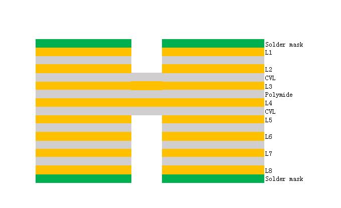
Rigid flex pcb layer stackup
Understanding The Basics Of Rigid Flex PCB Layer Stackup
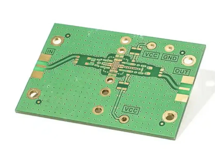
Rigid flex printed circuit boards (PCBs) represent a sophisticated amalgamation of rigid and flexible substrates, designed to meet the demands of modern electronic devices.
Understanding the basics of rigid flex PCB layer stackup is crucial for engineers and designers aiming to optimize the performance and reliability of their electronic products. The layer stackup in rigid flex PCBs is a critical aspect that influences the electrical, mechanical, and thermal properties of the final product.
To begin with, rigid flex PCBs consist of multiple layers of conductive and insulating materials.
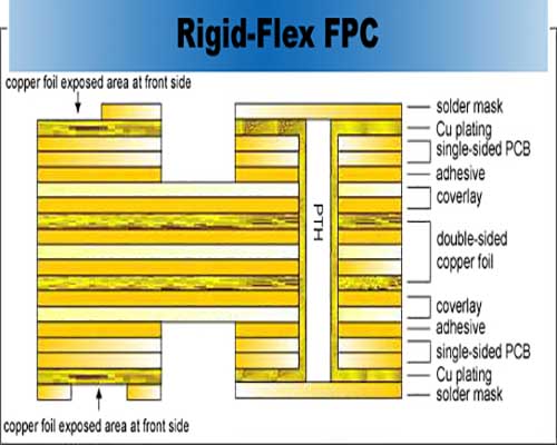
These layers are strategically arranged to achieve the desired electrical connectivity and mechanical flexibility. The rigid sections provide structural support and house components that require a stable platform, while the flexible sections allow for bending and folding, facilitating compact and complex designs. The transition between rigid and flexible sections must be meticulously planned to ensure seamless integration and functionality.
One of the primary considerations in rigid flex PCB layer stackup is the selection of materials.
The rigid sections typically use materials like FR4, a glass-reinforced epoxy laminate known for its excellent mechanical strength and thermal stability. On the other hand, the flexible sections often employ polyimide, a material renowned for its flexibility, thermal resistance, and dielectric properties. The choice of materials directly impacts the performance and durability of the PCB, making it essential to select materials that meet the specific requirements of the application.
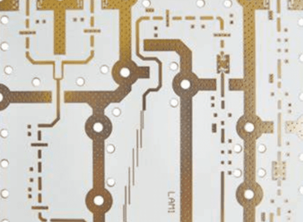
Another critical aspect is the arrangement of conductive layers.
In a typical rigid flex PCB, the conductive layers are made of copper and are interspersed with insulating layers. The number of conductive layers can vary depending on the complexity of the circuit and the design requirements. For instance, a simple design may have just a few layers, while more complex designs can have ten or more layers. The arrangement of these layers must be carefully planned to ensure optimal signal integrity, power distribution, and thermal management.
Furthermore, the transition zones between rigid and flexible sections require special attention.
These zones are often subjected to mechanical stress due to bending and flexing, which can lead to potential failure if not properly designed. To mitigate this risk, designers often use techniques such as staggered layer transitions, where the conductive layers in the flexible section are gradually tapered into the rigid section. This approach helps distribute the mechanical stress more evenly, enhancing the durability of the PCB.
In addition to material selection and layer arrangement, the manufacturing process also plays a vital role in the quality of the rigid flex PCB. Advanced fabrication techniques, such as laser drilling and precision etching, are employed to create the intricate patterns and vias required for complex designs. These processes must be executed with high precision to ensure the integrity of the electrical connections and the overall reliability of the PCB.
Moreover, testing and validation are essential steps in the development of rigid flex PCBs. Rigorous testing, including electrical, mechanical, and thermal assessments, helps identify potential issues and ensures that the PCB meets the required performance standards. This comprehensive approach to testing is crucial for applications where reliability is paramount, such as in aerospace, medical devices, and consumer electronics.
In conclusion, understanding the basics of rigid flex PCB layer stackup involves a thorough consideration of material selection, layer arrangement, transition zone design, manufacturing processes, and testing protocols. By meticulously addressing these factors, engineers and designers can create robust and reliable rigid flex PCBs that meet the demanding requirements of modern electronic applications.
Key Design Considerations For Rigid Flex PCB Layer Stackup
When designing a rigid-flex PCB layer stackup, several key considerations must be taken into account to ensure optimal performance and reliability. One of the primary factors to consider is the material selection.
The materials used in rigid-flex PCBs must be compatible with both the rigid and flexible sections of the board. Typically, FR4 is used for the rigid sections, while polyimide is preferred for the flexible areas due to its excellent thermal stability and flexibility. The choice of materials directly impacts the board’s mechanical and thermal properties, which are crucial for its performance in various applications.
Another critical aspect is the layer configuration.
The number of layers in a rigid-flex PCB can vary depending on the complexity of the design and the specific requirements of the application. It is essential to carefully plan the layer stackup to ensure proper signal integrity and minimize electromagnetic interference (EMI). This involves strategically placing ground and power planes, as well as signal layers, to achieve the desired electrical performance. Additionally, the layer stackup must be designed to accommodate the bending and flexing of the flexible sections without causing damage to the traces or vias.
The thickness of the layers is also a significant consideration.
The overall thickness of the rigid-flex PCB must be carefully controlled to ensure it meets the mechanical requirements of the application. This includes considering the thickness of the copper layers, dielectric materials, and any additional adhesive layers. The thickness of the flexible sections must be minimized to allow for easy bending and flexing, while the rigid sections must be thick enough to provide the necessary structural support. Balancing these requirements is crucial to achieving a reliable and functional rigid-flex PCB.
Furthermore, the design of the transition areas between the rigid and flexible sections is of utmost importance.
These transition areas are often the most vulnerable points in a rigid-flex PCB, as they are subjected to mechanical stress during bending and flexing. To mitigate the risk of failure, it is essential to use appropriate design techniques, such as staggered vias and filleted corners, to distribute the stress more evenly. Additionally, the use of reinforcements, such as stiffeners or strain reliefs, can help protect the transition areas and enhance the overall durability of the board.
Thermal management is another key consideration in rigid-flex PCB design.
The materials used in the board must be able to withstand the thermal cycling and heat dissipation requirements of the application. This involves selecting materials with appropriate thermal conductivity and coefficient of thermal expansion (CTE) properties. Proper thermal management is essential to prevent issues such as delamination, warping, and thermal fatigue, which can compromise the performance and reliability of the rigid-flex PCB.
Lastly, manufacturability and cost are important factors to consider.
The design of the rigid-flex PCB layer stackup must be optimized for efficient manufacturing processes to minimize production costs and lead times. This includes considering factors such as panel utilization, material waste, and the complexity of the assembly process. Collaborating with experienced PCB manufacturers during the design phase can help identify potential manufacturing challenges and ensure a cost-effective and reliable final product.
In conclusion, designing a rigid-flex PCB layer stackup involves careful consideration of material selection, layer configuration, thickness control, transition area design, thermal management, and manufacturability. By addressing these key factors, designers can create robust and reliable rigid-flex PCBs that meet the specific requirements of their applications.
Common Challenges In Rigid Flex PCB Layer Stackup And How To Overcome Them
Rigid flex PCBs, which combine the benefits of both rigid and flexible circuit boards, are increasingly popular in various high-performance applications. However, designing and manufacturing these complex structures come with their own set of challenges, particularly in the layer stackup process. Understanding these challenges and how to overcome them is crucial for ensuring the reliability and functionality of the final product.
One of the primary challenges in rigid flex PCB layer stackup is managing the different material properties.
Rigid sections typically use FR4, a glass-reinforced epoxy laminate, while flexible sections use polyimide, a material known for its flexibility and thermal stability. These materials have different coefficients of thermal expansion (CTE), which can lead to mechanical stress and potential delamination during thermal cycling. To mitigate this issue, designers must carefully select materials with compatible CTE values and employ advanced simulation tools to predict and manage thermal stresses.
Another significant challenge is ensuring signal integrity across the rigid and flexible sections.
The transition between these sections can introduce impedance discontinuities, which can degrade signal quality. To address this, designers should use controlled impedance techniques and carefully plan the layer stackup to maintain consistent impedance throughout the circuit. Additionally, incorporating ground planes and using differential pairs can help minimize signal loss and crosstalk.
The mechanical reliability of the flexible sections is also a concern, particularly in applications that involve repeated bending or flexing.
Over time, mechanical stress can lead to cracks or breaks in the conductive traces. To enhance durability, designers can use staggered or serpentine trace patterns, which distribute stress more evenly and reduce the likelihood of failure. Furthermore, selecting appropriate coverlay materials and thicknesses can provide additional protection to the flexible sections.
Manufacturing tolerances present another challenge in rigid flex PCB layer stackup.
The precise alignment of multiple layers is critical for ensuring electrical connectivity and mechanical integrity. Misalignment can result in open circuits or short circuits, compromising the functionality of the PCB. To overcome this, manufacturers should employ high-precision equipment and rigorous quality control processes. Additionally, incorporating fiducial markers and alignment features in the design can aid in accurate layer registration during fabrication.
Cost considerations also play a significant role in the design and manufacturing of rigid flex PCBs.
The complexity of the layer stackup, combined with the need for specialized materials and processes, can drive up production costs. To manage expenses, designers should optimize the layer count and minimize the use of expensive materials where possible. Collaborating closely with manufacturers during the design phase can also help identify cost-saving opportunities without compromising performance.
Finally, ensuring proper thermal management is essential for the reliable operation of rigid flex PCBs, especially in high-power applications.
The combination of rigid and flexible sections can create hotspots, leading to thermal stress and potential failure. Effective thermal management strategies include using thermal vias, heat sinks, and appropriate layer stackup configurations to dissipate heat efficiently. Conducting thermal simulations during the design phase can help identify potential issues and optimize the thermal performance of the PCB.
In conclusion, while rigid flex PCB layer stackup presents several challenges, understanding these issues and implementing appropriate design and manufacturing strategies can significantly enhance the reliability and performance of the final product. By carefully managing material properties, ensuring signal integrity, enhancing mechanical reliability, maintaining manufacturing tolerances, controlling costs, and optimizing thermal management, designers and manufacturers can successfully navigate the complexities of rigid flex PCB layer stackup.
Innovations And Trends In Rigid Flex PCB Layer Stackup Technology
Rigid flex PCB layer stackup technology has undergone significant advancements in recent years, driven by the increasing demand for more compact, reliable, and versatile electronic devices. This technology, which combines the benefits of both rigid and flexible circuit boards, has become a cornerstone in the design and manufacturing of modern electronics. As the industry continues to evolve, several innovations and trends have emerged, shaping the future of rigid flex PCB layer stackup technology.
One of the most notable innovations in this field is the development of advanced materials.
Traditional rigid flex PCBs were primarily constructed using polyimide films and epoxy resins. However, recent advancements have introduced new materials such as liquid crystal polymers (LCPs) and thermoplastic polyimides. These materials offer superior thermal stability, mechanical strength, and electrical performance, making them ideal for high-frequency applications and harsh environments. The use of these advanced materials has enabled the creation of more robust and reliable rigid flex PCBs, capable of withstanding the demands of modern electronic devices.
In addition to material advancements, the design and manufacturing processes of rigid flex PCBs have also seen significant improvements.
One such trend is the adoption of high-density interconnect (HDI) technology. HDI technology allows for the creation of PCBs with finer lines and spaces, smaller vias, and higher layer counts. This results in increased circuit density and improved electrical performance, which are essential for the miniaturization of electronic devices. The integration of HDI technology into rigid flex PCB layer stackup designs has enabled manufacturers to produce more compact and efficient circuit boards, meeting the ever-growing demand for smaller and more powerful electronic devices.
Another important trend in rigid flex PCB layer stackup technology is the emphasis on environmental sustainability.
As the electronics industry faces increasing pressure to reduce its environmental impact, manufacturers are exploring eco-friendly materials and processes. For instance, the use of lead-free solder and halogen-free laminates has become more prevalent in rigid flex PCB manufacturing. Additionally, advancements in recycling and waste management techniques have allowed for the more efficient recovery and reuse of materials, further reducing the environmental footprint of rigid flex PCBs.
The rise of the Internet of Things (IoT) and wearable technology has also played a significant role in shaping the future of rigid flex PCB layer stackup technology.
These applications require highly flexible and durable circuit boards that can withstand constant bending and flexing. As a result, manufacturers are developing new techniques to enhance the flexibility and durability of rigid flex PCBs. For example, the use of stretchable conductive materials and innovative layering techniques has enabled the creation of PCBs that can maintain their performance even under extreme mechanical stress. This has opened up new possibilities for the design and functionality of IoT devices and wearables, driving further innovation in the field.
Moreover, the increasing complexity of electronic devices has led to the need for more sophisticated testing and quality assurance methods.
Advanced inspection techniques, such as automated optical inspection (AOI) and X-ray inspection, have become essential in ensuring the reliability and performance of rigid flex PCBs. These methods allow for the detection of defects and inconsistencies at various stages of the manufacturing process, ensuring that the final product meets the highest standards of quality and performance.
In conclusion, the innovations and trends in rigid flex PCB layer stackup technology are driving the evolution of modern electronics. The development of advanced materials, the adoption of HDI technology, the focus on environmental sustainability, and the rise of IoT and wearable technology are all contributing to the advancement of this field. As the demand for more compact, reliable, and versatile electronic devices continues to grow, rigid flex PCB layer stackup technology will undoubtedly play a crucial role in meeting these challenges and shaping the future of electronics.