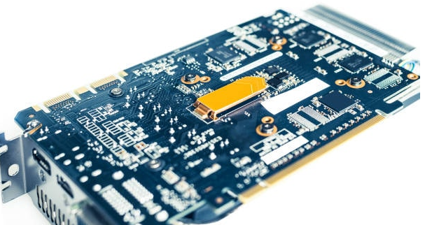
Risk factors that PCB board reliability should avoid!
Whether it is in the manufacturing assembly process or in actual use, it is essential that the PCB has reliable performance.
In addition to the associated costs, defects in the assembly process may be carried into the final product by the PCB,
and failure may occur during actual use, resulting in a claim. Therefore, from this point of view,
it is no exaggeration to say that the cost of a good quality PCB is negligible. In all market segments,
especially in markets where products for critical applications are produced, the consequences of such failures are unimaginable.
These aspects should be kept in mind when comparing PCB prices and looking for PCB processing. Although the initial cost of a reliable, guaranteed, and long-life product is high, it is worth the money in the long run. Let’s take a look at the 14 most important features of a highly reliable board:
1, 25-micron hole wall copper thickness
Benefits: Enhanced reliability, including improved z-axis resistance to expansion.
The risk of not doing this: lowing or degassing electrical connectivity problems during assembly (inner layer separation, hole wall fracture), or failure under load conditions in actual use. IPCClass2 (the standard used in most plants) requires 20% less copper plating.
2, no welding repair or open circuit repair
Benefits: Perfect circuit ensures reliability and safety, no maintenance, no risk
Risk of not doing so
If it is not repaired properly, it will cause the board to open. Even if the repair is ‘proper’, there is a risk of failure under load conditions (vibration, etc.), which may cause a malfunction in actual use.

3, Exceeding the cleanliness requirements of the IPC specification
Benefits: Improve PCB cleanliness to increase reliability.
Risk of not doing so
Residues and solder deposits on the board pose a risk to the solder mask. Ion residues can cause corrosion and contamination risks on the soldered surface, which can lead to reliability issues (bad solder joints/electrical faults) and ultimately increase the actual fault occurrence. Probability.
4, Strictly control the service life of each surface treatment
Benefits: solderability, reliability, and reduced risk of moisture intrusion
Risk of not doing so
Due to metallographic changes in the surface treatment of old boards, soldering problems may occur, and moisture intrusion may cause delamination, separation of inner layers and walls (opening) during assembly and/or actual use…
5, Use internationally renowned substrates – do not use “local” or unknown brands
Benefits: Improve reliability and known performance
Risk of not doing so
Poor mechanical properties mean that the board does not perform as expected under assembly conditions. For example, high expansion performance can cause delamination, open circuit, and warpage problems. Impaired electrical characteristics can result in poor impedance performance.
6, Cladding tolerance meets IPC4101 Class B/L requirements
Benefits: Strict control of the dielectric layer thickness can reduce the expected deviation of electrical performance.
Risk of not doing so
Electrical performance may not meet the specified requirements, and the output/performance of the same batch of components will vary greatly.
7, Define the solder mask material to ensure compliance with IPC-SM-840 ClassT requirements
Benefits: “Excellent” inks for ink safety and ensuring solder mask inks meet UL standards.
Risk of not doing so
Inferior inks can cause adhesion, flux resistance, and hardness problems. All of these problems can cause the solder mask to detach from the board and eventually lead to corrosion of the copper circuit. Poor insulation properties can cause short circuits due to unexpected electrical connectivity/arc.
8, Define tolerances for shapes, holes and other mechanical features
Benefits: Strict control of tolerances can improve the dimensional quality of the product – improved fit, shape, and function
Risk of not doing so
Problems during assembly, such as alignment/mating (the problem of press-fit needles is only found when the assembly is complete). In addition, there is a problem in mounting the base due to an increase in dimensional deviation.
9, Requirements for solder mask thickness, although IPC has no relevant regulations
Benefits: Improve electrical insulation properties, reduce the risk of flaking or loss of adhesion, and strengthen the ability to withstand mechanical impact – no matter where the mechanical impact occurs!
Risk of not doing so
Thin solder masks can cause adhesion, flux resistance, and hardness problems. All of these problems can cause the solder mask to detach from the board and eventually lead to corrosion of the copper circuit. Poor insulation properties due to the thin solder mask layer can cause short circuits due to accidental conduction/arc.
10, Define appearance requirements and repair requirements, although IPC is not defined
Benefits: Care and careful care in the manufacturing process.
Risk of not doing so
A variety of scratches, minor injuries, repairs, and repairs – the board can be used but not good looking. In addition to the problems that the surface can see, what are the invisible risks, the impact on assembly, and the risks in actual use?
11, the requirements for plug depth
Benefit: High-quality plug holes will reduce the risk of failure during assembly.
Risk of not doing so
The chemical residue in the gold sinking process may remain in the hole that is not filled with the plug hole,
thereby causing problems such as solderability. Moreover, tin beads may be hidden in the holes, and the solder balls may splash out during assembly or actual use, causing a short circuit.
12, specify the peelable blue plastic brand and model
Benefit: The designation of peelable blue glue avoids the use of “local” or cheap brands.
Risk of not doing so
Inferior or inexpensive peelable glue may foam, melt, crack or solidify like concrete during assembly so that the peelable glue cannot be peeled off/inactive.
13, Perform specific approval and order procedures for each purchase order
Benefits: The execution of this program ensures that all specifications have been confirmed.
Risk of not doing so
If the product specifications are not carefully confirmed, the resulting deviation may not be discovered until the assembly or final product, and it is too late.
14, Do not accept sets of boards with scrapped units
Benefits: No partial assembly can help customers improve efficiency.
Risk of not doing so
A defective assembly requires a special assembly procedure. If the x-out is not clearly marked or is not isolated from the panel, it is possible to assemble the known bad plate. Waste parts and time.
Alice Lu
Email: sales16@andwinpcb.com