Secure Computer PCB Cloning and Custom Development: A Comprehensive Guide
Introduction
Printed Circuit Board (PCB) cloning and custom development are critical processes in the electronics industry, particularly in the fields of secure computing, embedded systems, and industrial automation. PCB cloning involves reverse-engineering an existing board to create an identical or improved version, while custom PCB development focuses on designing new boards tailored to specific requirements.
In secure computing, ensuring the integrity, confidentiality, and reliability of PCBs is paramount. This article explores the methodologies, challenges, and best practices in secure computer PCB cloning and custom development, covering key aspects such as reverse engineering, design optimization, security considerations, and compliance with industry standards.
1. Understanding PCB Cloning
1.1 What is PCB Cloning?
PCB cloning, also known as PCB copying or reverse engineering, is the process of analyzing an existing circuit board to replicate its design. This is often done to:
- Replace obsolete or discontinued boards.
- Improve existing designs (e.g., enhancing signal integrity or thermal performance).
- Conduct security audits and vulnerability assessments.
- Develop compatible or upgraded versions of legacy systems.
1.2 The PCB Cloning Process
The typical workflow for PCB cloning includes:
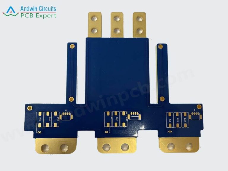
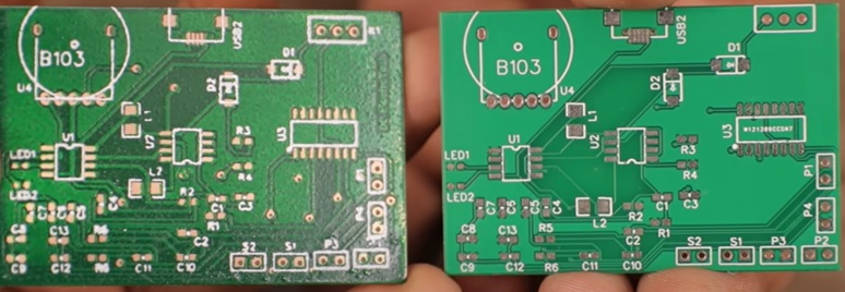
Step 1: Physical Inspection and Documentation
- High-resolution imaging of the PCB (top and bottom layers).
- Identifying key components (ICs, resistors, capacitors, connectors).
- Recording layer stack-up and material properties.
Step 2: Schematic Extraction
- Tracing connections using multimeters and continuity testers.
- Using specialized software (e.g., Altium, KiCad, Eagle) to reconstruct the schematic.
- Verifying signal paths and power distribution.
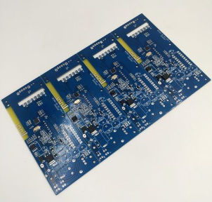
Step 3: PCB Layout Recreation
- Replicating the board layout while optimizing for manufacturability.
- Adjusting trace widths, spacing, and impedance matching if needed.
- Generating Gerber files for fabrication.
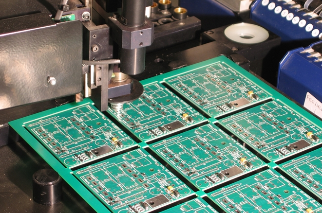
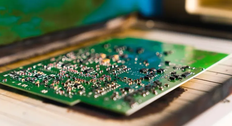
Step 4: Prototyping and Testing
- Manufacturing a prototype PCB.
- Functional testing to ensure performance matches the original.
- Debugging and refining the design.
2. Secure PCB Cloning: Challenges and Countermeasures
2.1 Security Risks in PCB Cloning
While cloning can be beneficial, it also poses security risks:
- Intellectual Property (IP) Theft: Unauthorized duplication of proprietary designs.
- Hardware Trojans: Malicious modifications during reverse engineering.
- Side-Channel Attacks: Extracting sensitive data through power analysis or electromagnetic leaks.
2.2 Mitigation Strategies
To ensure secure PCB cloning:
- Use Obfuscation Techniques: Hidden traces, dummy components, or encrypted firmware.
- Implement Secure Boot: Prevent unauthorized firmware execution.
- Employ Tamper-Resistant Designs: Anti-reverse engineering coatings, epoxy encapsulation.
- Adopt Hardware Authentication: Secure elements (e.g., TPM, HSMs) to verify board legitimacy.
3. Custom PCB Development for Secure Computing
3.1 Key Considerations in Custom PCB Design
When developing custom PCBs for secure applications, engineers must address:
- Signal Integrity: Minimizing noise and crosstalk in high-speed designs.
- Power Integrity: Stable voltage regulation and decoupling.
- Thermal Management: Efficient heat dissipation for reliability.
- EMI/EMC Compliance: Reducing electromagnetic interference.
3.2 Security-Focused Design Practices
To enhance security:
- Partitioning Critical Circuits: Isolate sensitive components (e.g., cryptographic modules).
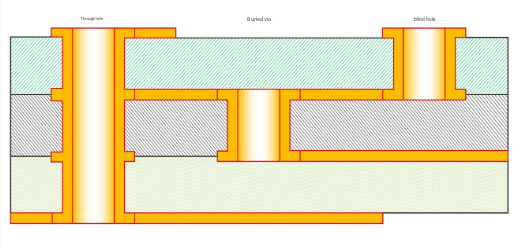
- Secure PCB Layers: Use buried vias and internal ground planes to prevent probing.
- Firmware Protection: Secure boot, encrypted storage, and runtime integrity checks.
- Supply Chain Security: Source components from trusted vendors to avoid counterfeit parts.
4. Industry Standards and Compliance
Secure PCB development must adhere to industry standards such as:
- ISO/IEC 15408 (Common Criteria): For hardware security evaluation.
- NIST SP 800-193: Guidelines for firmware resilience.
- IPC Standards: IPC-2221 (generic PCB design), IPC-7351 (component spacing).
- GDPR & CCPA: Data protection regulations affecting embedded systems.
5. Case Study: Secure Military-Grade PCB Development
A defense contractor required a secure, tamper-proof PCB for a military communication device. The solution involved:
- Multi-layer PCB with embedded security features (shielded traces, tamper detection).
- Hardware-based encryption using FPGAs with bitstream protection.
- Rigorous penetration testing to validate resistance against physical and side-channel attacks.
The final design met NSA Type-1 certification requirements, demonstrating the effectiveness of secure PCB methodologies.
6. Future Trends in Secure PCB Technology
Emerging advancements include:
- AI-Assisted PCB Design: Automated optimization for security and performance.
- Quantum-Resistant Cryptography: Future-proofing secure hardware.
- 3D-Printed Electronics: Rapid prototyping with embedded security features.
- Blockchain for Supply Chain Verification: Ensuring component authenticity.
Conclusion
Secure computer PCB cloning and custom development require a balance between functionality, manufacturability, and security. By following best practices—such as secure design principles, anti-tamper mechanisms, and compliance with industry standards—engineers can develop robust PCBs for critical applications. As technology evolves, integrating AI, quantum security, and trusted manufacturing processes will further enhance PCB security.