Selecting Expert HDI PCB Suppliers for Cost-Effective Designs
Key Takeaways
When evaluating HDI PCB suppliers, prioritize expertise in advanced manufacturing techniques that directly impact PCB manufacturing cost and product reliability. Top-tier PCB manufacturing companies leverage laser-drilled microvias to minimize layer counts while maintaining signal integrity—a critical factor for compact designs. Verify compliance with IPC-2226 standards to ensure robust via structures and material selection, which prevent costly redesigns or field failures.
Cost optimization extends beyond raw materials: skilled suppliers analyze stackup configurations to balance performance needs with PCB manufacturing business economics. For instance, combining blind/buried vias with through-holes can reduce layer transitions by 30–40%, directly lowering assembly complexity. Always request design-for-manufacturability (DFM) feedback early—experienced partners identify layout inefficiencies that inflate PCB manufacturing expenses.
Finally, assess suppliers’ capacity for rapid prototyping and scalable production. Time-to-market pressures demand seamless transitions from prototype to volume runs, a capability distinguishing leaders in HDI PCB manufacturing. By aligning technical rigor with cost-conscious strategies, you secure both performance and profitability.
HDI PCB Supplier Selection Criteria
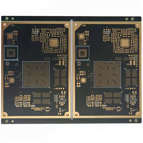
When evaluating HDI PCB suppliers, you need to prioritize technical expertise that aligns with your project’s complexity. Start by verifying their experience in pcb manufacturing for high-density designs, particularly their ability to handle laser-drilled microvias and stacked via configurations. Reputable pcb manufacturing companies often showcase certifications like IPC-2226 compliance, which ensures adherence to design standards for HDI reliability.
| Key Evaluation Factor | Impact on Selection |
|---|---|
| Microvia Technology Mastery | Enables compact layouts, reducing pcb manufacturing cost |
| Material Sourcing Networks | Lowers component expenses without sacrificing performance |
| DFM (Design for Manufacturing) Support | Optimizes layer stackups for cost efficiency |
Tip: Always request a design review before finalizing your supplier. This step uncovers potential cost traps in material selection or layer counts, especially for high-mix pcb manufacturing business models.
Second, assess their scalability. Suppliers with automated processes for impedance control and plating uniformity typically deliver better yields, which directly impacts pcb manufacturing cost over time. Don’t overlook their track record in thermal management solutions—critical for avoiding field failures in dense designs. For deeper insights into HDI material selection, explore [this guide]() on advanced substrate options.
Finally, prioritize partners who transparently break down cost drivers, from blind/buried via structures to surface finishes. Transparent pricing models help you balance performance needs with budget constraints, ensuring your HDI project stays competitive without compromising quality.
Cost Drivers in HDI PCB Production
When evaluating PCB manufacturing costs for high-density interconnect designs, four primary factors dominate: material selection, layer complexity, via formation methods, and compliance requirements. Advanced substrates like high-Tg FR-4 or polyimide resins typically account for 25–35% of total expenses, as they ensure signal integrity in compact layouts. PCB manufacturing companies specializing in HDI often leverage laser-drilled microvias to minimize layer counts, but balancing stackup complexity against fabrication tolerances remains critical—each additional layer increases PCB manufacturing business overhead by 8–12%.
Via structures also impact budgets: staggered or stacked microvias reduce board area but require precise laser systems, while through-holes demand more material and limit routing density. Compliance with standards like IPC-2226 adds 10–15% to testing costs but prevents field failures, making it a non-negotiable investment. To optimize PCB manufacturing cost, prioritize suppliers offering design-for-manufacturability (DFM) analysis early in prototyping—this avoids late-stage revisions that inflate timelines by 3–5 weeks. By aligning your design goals with a supplier’s process capabilities, you mitigate risks while maintaining performance thresholds.
Microvia Tech for Compact PCB Designs
When optimizing for space-constrained applications, microvia technology becomes critical in balancing performance and PCB manufacturing cost. Unlike traditional through-holes, microvias—laser-drilled interconnects with diameters under 150µm—enable higher-density routing while minimizing layer counts. This directly impacts material usage and assembly complexity, two key drivers in PCB manufacturing business profitability.
Leading PCB manufacturing companies leverage microvias to achieve aspect ratios of 1:1 or better, supporting designs with 0.4mm pitch BGAs or finer. By integrating staggered or stacked microvias, you can reduce signal path lengths, enhancing electrical performance without inflating layer stackups. However, process precision is non-negotiable: improper laser drilling or plating can compromise reliability, escalating long-term costs.
For cost-sensitive projects, consider hybrid approaches—combining microvias with selective through-holes—to maintain signal integrity in critical areas while using standard vias elsewhere. This strategy aligns with PCB manufacturing best practices, ensuring yield optimization without over-engineering. Always verify supplier capabilities in microvia fabrication, as inconsistent quality among vendors can lead to hidden PCB manufacturing cost spikes from rework or scrap.
By prioritizing suppliers with proven microvia expertise, you ensure designs remain compact, functional, and economically viable across production scales.
IPC-2226 Compliance in HDI Manufacturing
When evaluating PCB manufacturing companies for HDI projects, understanding IPC-2226 compliance becomes critical. This standard governs the design and reliability requirements for high-density interconnect (HDI) boards, ensuring they meet performance benchmarks in demanding applications. Suppliers adhering to IPC-2226 demonstrate expertise in managing PCB manufacturing cost while maintaining quality, as the specification dictates precise material selection, layer alignment, and via formation.
For instance, the standard mandates strict tolerances for microvia aspect ratios (typically 1:1), which directly impacts PCB manufacturing feasibility. Expert suppliers optimize laser drilling parameters and dielectric materials to achieve these ratios without compromising yield rates. Additionally, IPC-2226’s thermal management guidelines prevent delamination risks in multilayer stacks—a common cost driver in PCB manufacturing business if unaddressed.
By prioritizing compliance, you gain assurance that critical parameters—like copper plating uniformity and impedance control—are systematically validated. This reduces post-production failures and aligns with cost-efficient scaling. However, not all suppliers invest in the advanced testing equipment required for full compliance. Partnering with certified manufacturers ensures your designs meet both technical and budgetary goals, avoiding hidden expenses from rework or material waste.
Optimizing HDI Layer Stackup Costs
When designing high-density interconnect (HDI) boards, your PCB manufacturing cost hinges significantly on layer stackup optimization. Balancing performance requirements with budget constraints requires strategic planning of layer counts, material choices, and via structures. Advanced HDI designs often demand more layers to accommodate complex routing, but every additional layer escalates raw material expenses and processing time. PCB manufacturing companies specializing in HDI solutions typically recommend starting with a thorough signal integrity analysis to identify the minimum viable layer count without compromising functionality.
A critical cost driver lies in sequential lamination cycles. While staggered microvias reduce layer counts by enabling vertical interconnects, multiple lamination steps increase production complexity. Partnering with PCB manufacturing experts helps determine whether combining blind/buried vias with through-holes can achieve similar performance at lower costs. For instance, using laser-drilled microvias in place of mechanical drilling minimizes material waste and reduces layer transitions.
Material selection also plays a pivotal role. Standard FR-4 substrates may suffice for lower-layer designs, but high-speed applications often require specialized laminates. PCB manufacturing business leaders emphasize aligning dielectric materials with your design’s thermal and electrical needs to avoid over-engineering. Transitioning to hybrid stackups—mixing high-performance and standard materials—can trim costs by 15–20% while maintaining reliability.
By collaborating closely with suppliers early in the design phase, you ensure that layer stackup decisions account for both technical specifications and PCB manufacturing cost targets. This proactive approach prevents costly redesigns and accelerates time-to-market for compact, high-performance solutions.
Microvias vs Through-Holes: Cost Analysis
When evaluating PCB manufacturing costs, the choice between microvias and through-holes significantly impacts your project’s budget. While traditional through-holes use mechanical drilling to create connections between layers, microvias employ laser-drilled technology to achieve finer geometries. For high-density designs, PCB manufacturing companies often recommend microvias due to their ability to reduce layer counts—a critical factor in minimizing PCB manufacturing business expenses. Though microvias require advanced equipment and stricter process controls (increasing initial setup costs), their precision enables tighter routing, potentially lowering material usage and improving yield rates in complex designs.
Through-holes, while simpler to produce, consume more board space and may necessitate additional layers to accommodate signal integrity requirements. This can escalate PCB manufacturing costs in multilayer designs, especially when paired with high-frequency applications. However, for less complex boards, through-holes remain cost-effective due to lower per-unit drilling expenses. To optimize spending, work with suppliers who analyze your design’s via density and aspect ratios to balance technology choices. By aligning fabrication methods with performance needs, you avoid over-engineering while maintaining compliance with standards like IPC-2226—a strategy expert PCB manufacturing partners prioritize for cost-efficient outcomes.
Ensuring HDI Reliability With Expert Suppliers
When partnering with PCB manufacturing companies specializing in high-density interconnect (HDI) designs, reliability hinges on their ability to balance technical precision with robust quality controls. Advanced PCB manufacturing processes, such as laser-drilled microvias and sequential lamination, require suppliers to maintain strict tolerances—often below 25µm—to prevent defects like via cracking or copper fatigue. Reputable suppliers implement design-for-reliability (DFR) methodologies, leveraging simulation tools to predict thermal stress and signal integrity issues before production begins.
To mitigate PCB manufacturing cost risks, experts optimize material selection—for example, pairing low-loss dielectrics with cost-effective copper weights—while adhering to IPC-2226 standards for HDI layer alignment. They also deploy automated optical inspection (AOI) and cross-sectional analysis to catch flaws in microvia fill quality or plating uniformity. By integrating reliability testing (e.g., thermal cycling, IST) into their PCB manufacturing business workflows, suppliers ensure boards withstand real-world operating conditions without compromising performance.
Choosing a partner with proven HDI expertise not reduces field failures but aligns with long-term cost efficiency. Their ability to troubleshoot signal crosstalk or impedance mismatches during prototyping phases minimizes redesign cycles, ensuring your final product meets both technical and budgetary goals.
Streamlining HDI PCB Time-to-Market
Reducing development cycles for HDI PCBs requires aligning design intent with pcb manufacturing capabilities early in the process. By collaborating with experienced pcb manufacturing companies, you can leverage design-for-manufacturability (DFM) feedback to avoid costly revisions. For instance, optimizing pad sizes or via placement based on a supplier’s laser drilling tolerances ensures fewer respins, directly lowering pcb manufacturing cost while accelerating prototyping.
Advanced suppliers integrate automated optical inspection (AOI) and real-time production tracking to minimize delays. This is critical in pcb manufacturing business models where shorter lead times translate to competitive advantages. Transitioning from traditional through-hole to microvia-dominated designs also cuts layer counts, reducing material waste and lamination cycles. However, balancing complexity with yield rates demands expertise—partnering with suppliers skilled in sequential lamination and blind/buried via integration ensures reliability without inflating timelines.
Finally, standardized material kits and pre-qualified stackups offered by leading manufacturers eliminate weeks of qualification testing. By synchronizing your design workflow with a supplier’s production pipeline, you compress time-to-market while maintaining compliance with IPC-2226 density benchmarks—a strategic approach for cost-sensitive, high-performance applications.
Conclusion
When finalizing your partnership with PCB manufacturing companies, it’s critical to recognize how strategic supplier selection directly impacts both PCB manufacturing cost and end-product performance. Expert suppliers leverage advanced microvia technology and IPC-2226 compliance to balance miniaturization demands with reliability, ensuring your high-density designs meet rigorous standards without unnecessary overhead. By prioritizing suppliers with proven expertise in layer stackup optimization and microvia drilling precision, you gain access to scalable solutions that align with evolving project requirements.
A key advantage lies in aligning your PCB manufacturing business goals with suppliers who transparently address cost drivers—from material selection to production scalability. When evaluating partners, focus on their ability to streamline prototyping cycles and reduce time-to-market through efficient design-for-manufacturing (DFM) practices. This approach not only minimizes PCB manufacturing cost but also mitigates risks associated with complex HDI layouts.
Ultimately, the right supplier acts as an extension of your engineering team, offering data-driven insights to refine designs for cost efficiency while maintaining signal integrity. By integrating their technical mastery with your product vision, you secure a competitive edge in delivering compact, high-performance electronics without compromising quality.
Frequently Asked Questions
How do PCB manufacturing costs vary between standard and HDI designs?
HDI designs typically involve higher initial costs due to microvia technology and tighter tolerances, but expert PCB manufacturing companies offset this through optimized panel utilization and advanced stacking techniques. The long-term savings from reduced board size and improved reliability often justify the upfront investment.
What qualifications should you prioritize when evaluating suppliers?
Look for IPC-2226 compliance certifications, proven expertise in laser-drilled microvias, and transparent PCB manufacturing cost breakdowns. Reputable suppliers provide design-for-manufacturability (DFM) feedback to eliminate unnecessary layers or features.
Can HDI technology reduce time-to-market for complex designs?
Yes. Skilled PCB manufacturing business partners streamline prototyping with rapid-turn services and automated testing, minimizing revisions. Their familiarity with blind/buried vias ensures proper signal integrity validation early in the process.
How do material choices impact HDI reliability and pricing?
High-frequency laminates or low-loss dielectrics increase PCB manufacturing cost but enhance performance in RF applications. Trusted suppliers recommend cost-balanced materials that meet your electrical and thermal requirements without over-engineering.
Why partner with specialized HDI manufacturers instead of general PCB manufacturing companies?
Specialists minimize risks like via cracking or delamination through precision laser drilling and controlled impedance management. Their process controls for sequential lamination directly affect yield rates and long-term board durability.
Explore Custom HDI Solutions for Your Project
Ready to balance performance and PCB manufacturing cost? Please click here to connect with engineers who optimize layer stackups, material selection, and testing protocols for your specific design needs.