Semi-flex pcb
Advantages Of Using Semi-Flex PCBs In Modern Electronics
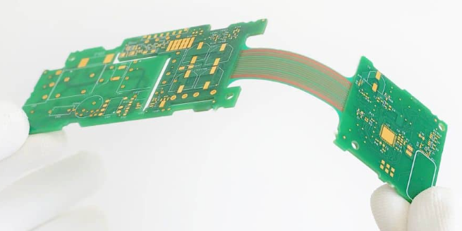
Semi-flex PCBs, or semi-flexible printed circuit boards, have emerged as a pivotal innovation in the realm of modern electronics. These hybrid boards combine the benefits of both rigid and flexible PCBs, offering a unique solution that addresses various design and functionality challenges. The advantages of using semi-flex PCBs in contemporary electronic devices are manifold, making them an increasingly popular choice among engineers and designers.
One of the primary advantages of semi-flex PCBs is their ability to reduce the overall size and weight of electronic devices.
By integrating flexible and rigid sections into a single board, designers can eliminate the need for connectors and cables that typically link separate rigid boards. This integration not only minimizes the space required but also reduces the weight, which is particularly beneficial in applications where compactness and portability are crucial, such as in wearable technology and portable medical devices.
In addition to size and weight reduction, semi-flex PCBs offer enhanced reliability.
The elimination of connectors and cables translates to fewer potential points of failure. Connectors are often susceptible to wear and tear, which can lead to intermittent connections or complete failure over time. By using a semi-flex PCB, the risk of such issues is significantly diminished, resulting in a more robust and dependable electronic device. This reliability is especially critical in high-stakes applications like aerospace and automotive industries, where failure is not an option.
Moreover, semi-flex PCBs provide greater design flexibility.
The ability to bend and flex certain sections of the board allows for more creative and efficient use of space within a device. This flexibility can be particularly advantageous in complex assemblies where traditional rigid boards would be impractical. For instance, in consumer electronics like smartphones and tablets, semi-flex PCBs can be designed to fit into tight spaces and around other components, optimizing the internal layout and improving overall performance.
Another significant benefit is the potential for cost savings.
While the initial manufacturing cost of semi-flex PCBs may be higher than that of traditional rigid boards, the long-term savings can be substantial. The reduction in the number of components, such as connectors and cables, simplifies the assembly process and reduces labor costs. Additionally, the enhanced reliability of semi-flex PCBs can lead to lower maintenance and repair costs over the lifespan of the device. This cost-effectiveness makes semi-flex PCBs an attractive option for a wide range of applications.
Furthermore, semi-flex PCBs contribute to improved signal integrity.
The direct connections within a semi-flex PCB reduce the chances of signal loss or interference, which can be a concern with traditional interconnects. This improved signal integrity is crucial in high-frequency applications, such as telecommunications and data transmission, where maintaining signal quality is paramount.
In conclusion, the advantages of using semi-flex PCBs in modern electronics are compelling. Their ability to reduce size and weight, enhance reliability, offer design flexibility, provide cost savings, and improve signal integrity makes them an invaluable asset in the development of contemporary electronic devices. As technology continues to advance and the demand for more compact, reliable, and efficient devices grows, the adoption of semi-flex PCBs is likely to increase, solidifying their role as a cornerstone in the future of electronics design and manufacturing.

Design Considerations For Semi-Flex PCBs
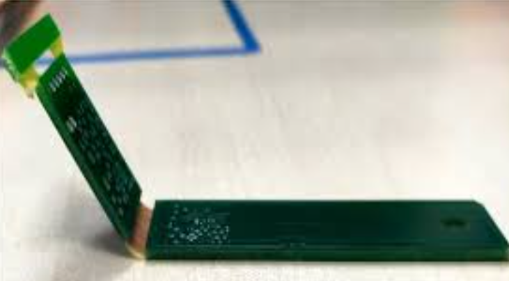
When designing semi-flex PCBs, several critical considerations must be taken into account to ensure optimal performance and reliability. Semi-flex PCBs, which combine the benefits of both rigid and flexible circuits, are increasingly popular in applications requiring a balance of durability and flexibility. The design process for these hybrid circuits involves meticulous planning and a deep understanding of the materials and manufacturing processes involved.
One of the primary considerations in designing semi-flex PCBs is the selection of appropriate materials.
The choice of materials significantly impacts the board’s flexibility, durability, and overall performance. Typically, semi-flex PCBs are constructed using a combination of rigid FR4 material and flexible polyimide. The rigid sections provide structural support, while the flexible sections allow for bending and movement. It is crucial to select materials that can withstand the mechanical stresses encountered during bending and flexing without compromising the electrical integrity of the circuit.
Another important factor is the thickness of the flexible sections.
The thickness must be carefully controlled to ensure that the board can bend without causing damage to the conductive traces or the insulating layers. Thinner flexible sections offer greater flexibility but may be more susceptible to mechanical damage. Conversely, thicker sections provide more durability but may limit the degree of flexibility. Therefore, finding the right balance between thickness and flexibility is essential for the successful implementation of semi-flex PCBs.
The layout and routing of traces in semi-flex PCBs also require special attention.
Designers must ensure that the traces in the flexible sections are routed in a manner that minimizes stress and potential damage during bending. This often involves using curved traces instead of sharp angles, as sharp angles can create stress points that may lead to cracking or breaking of the conductive material. Additionally, it is advisable to use wider traces in the flexible sections to distribute the mechanical stress more evenly and reduce the risk of trace failure.
Thermal management is another critical aspect of semi-flex PCB design.
The combination of rigid and flexible materials can create challenges in dissipating heat effectively. Designers must consider the thermal properties of both the rigid and flexible sections and ensure that adequate thermal management solutions are in place. This may involve the use of thermal vias, heat sinks, or other cooling mechanisms to prevent overheating and ensure the reliable operation of the circuit.
Furthermore, the manufacturing process for semi-flex PCBs requires careful consideration.
The process typically involves multiple steps, including the lamination of rigid and flexible materials, drilling, plating, and etching. Each step must be precisely controlled to ensure that the final product meets the required specifications. Any deviations in the manufacturing process can lead to defects such as delamination, misalignment, or incomplete etching, which can compromise the performance and reliability of the PCB.
In addition to these technical considerations, designers must also take into account the specific requirements of the application for which the semi-flex PCB is intended. This includes factors such as the operating environment, mechanical stresses, and electrical performance requirements.
By thoroughly understanding the application and its demands, designers can make informed decisions about the materials, layout, and manufacturing processes to ensure that the semi-flex PCB meets the necessary performance and reliability standards.
In conclusion, designing semi-flex PCBs involves a complex interplay of material selection, trace routing, thermal management, and manufacturing processes. By carefully considering these factors and understanding the specific requirements of the application, designers can create robust and reliable semi-flex PCBs that offer the desired balance of flexibility and durability.
Manufacturing Process Of Semi-Flex PCBs
The manufacturing process of semi-flex PCBs, a hybrid between rigid and flexible circuit boards, involves several intricate steps that ensure the final product meets the required specifications and performance standards. This process begins with the selection of appropriate materials, which is crucial for achieving the desired flexibility and durability. Typically, a semi-flex PCB is constructed using a combination of rigid FR4 material and flexible polyimide layers. The choice of materials directly impacts the board’s ability to withstand mechanical stress and environmental factors.
Once the materials are selected, the next step involves the preparation of the substrate.
This involves cleaning and treating the surface to ensure proper adhesion of subsequent layers. The substrate is then laminated with a copper foil, which serves as the conductive layer. This lamination process is carried out under controlled temperature and pressure conditions to ensure uniformity and prevent defects.
Following lamination, the copper foil is patterned using a photolithographic process.
This involves coating the copper surface with a photosensitive resist, exposing it to ultraviolet light through a photomask, and then developing the image. The exposed areas of the resist are hardened, while the unexposed areas are washed away, revealing the underlying copper. The exposed copper is then etched away using a chemical solution, leaving behind the desired circuit pattern.
After etching, the next step is the drilling process, where holes are created for vias and through-hole components.
These holes are drilled using precision machinery to ensure accuracy and alignment. Once the drilling is complete, the holes are plated with copper to establish electrical connections between different layers of the PCB.
The semi-flex PCB then undergoes a series of additional lamination steps to build up the required number of layers.
Each layer is carefully aligned and bonded under heat and pressure to form a cohesive structure. During this stage, the flexible regions of the PCB are created by selectively removing the rigid FR4 material, leaving behind the flexible polyimide sections. This selective removal is typically achieved through a controlled milling or laser cutting process.
Following the lamination and milling processes, the semi-flex PCB is subjected to a series of inspections and tests to ensure quality and reliability.
These inspections include visual checks, electrical testing, and mechanical stress tests. Any defects or inconsistencies are identified and rectified to ensure the final product meets the required standards.
The final steps in the manufacturing process involve the application of surface finishes and protective coatings.
Surface finishes, such as HASL (Hot Air Solder Leveling), ENIG (Electroless Nickel Immersion Gold), or OSP (Organic Solderability Preservative), are applied to the exposed copper surfaces to enhance solderability and protect against oxidation. Protective coatings, such as solder mask and conformal coating, are applied to shield the PCB from environmental factors and mechanical damage.
In conclusion, the manufacturing process of semi-flex PCBs is a complex and meticulous procedure that requires careful selection of materials, precise patterning, and rigorous testing. Each step is critical to ensuring the final product’s performance, reliability, and durability. By understanding and controlling these processes, manufacturers can produce high-quality semi-flex PCBs that meet the demanding requirements of modern electronic applications.
Applications Of Semi-Flex PCBs In Various Industries
Semi-flex PCBs, a hybrid between rigid and flexible printed circuit boards, have become increasingly popular due to their unique combination of flexibility and durability. These PCBs are designed to bend slightly, allowing for more versatile applications compared to their rigid counterparts. The semi-flex PCB’s ability to withstand mechanical stress while maintaining electrical performance makes it an ideal choice for various industries. This article explores the diverse applications of semi-flex PCBs across different sectors, highlighting their significance and advantages.
In the consumer electronics industry, semi-flex PCBs are widely used in devices that require compact and reliable circuitry.
Smartphones, tablets, and wearable technology benefit from the semi-flex PCB’s ability to fit into tight spaces while providing robust electrical connections. The slight flexibility of these PCBs allows for better shock absorption, which is crucial in portable devices that are frequently subjected to drops and impacts. Additionally, the semi-flex design enables manufacturers to create thinner and lighter products without compromising on performance, meeting the ever-growing demand for sleek and efficient consumer electronics.
Transitioning to the automotive industry, semi-flex PCBs play a critical role in modern vehicle design.
With the increasing integration of electronic systems in cars, from advanced driver-assistance systems (ADAS) to infotainment units, the need for reliable and durable PCBs has never been greater. Semi-flex PCBs are used in various automotive applications, including dashboard displays, engine control units, and lighting systems.
Their ability to withstand high temperatures and vibrations makes them suitable for the harsh conditions often encountered in automotive environments. Moreover, the semi-flex PCB’s adaptability allows for innovative design solutions, such as curved displays and compact control modules, enhancing both functionality and aesthetics in vehicles.
In the medical field, the demand for miniaturized and reliable electronic components has led to the adoption of semi-flex PCBs in medical devices.
These PCBs are used in diagnostic equipment, wearable health monitors, and implantable devices. The semi-flex PCB’s flexibility is particularly advantageous in medical applications where devices must conform to the human body’s contours or fit into small, intricate spaces. For instance, in wearable health monitors, the semi-flex PCB can bend to match the shape of the user’s wrist, ensuring comfort and continuous monitoring. Furthermore, the reliability and durability of semi-flex PCBs are essential in critical medical devices, where any failure could have serious consequences.
The aerospace industry also benefits from the unique properties of semi-flex PCBs.
In this sector, electronic systems must endure extreme conditions, including high altitudes, temperature fluctuations, and intense vibrations. Semi-flex PCBs are used in various aerospace applications, such as satellite systems, avionics, and communication equipment. Their ability to maintain performance under stress and their lightweight nature make them ideal for aerospace applications where weight and reliability are paramount. Additionally, the semi-flex PCB’s design flexibility allows for more efficient use of space within the confined environments of aircraft and spacecraft.
Lastly, the industrial sector leverages semi-flex PCBs in automation and control systems.
These PCBs are used in machinery, robotics, and industrial sensors, where they must withstand harsh operating conditions, including exposure to chemicals, moisture, and mechanical stress. The semi-flex PCB’s robustness and adaptability ensure reliable performance in demanding industrial environments, contributing to increased efficiency and reduced downtime.
In conclusion, semi-flex PCBs have found applications across a wide range of industries due to their unique combination of flexibility, durability, and reliability. From consumer electronics to automotive, medical, aerospace, and industrial sectors, these PCBs offer innovative solutions that enhance performance and design possibilities. As technology continues to advance, the demand for semi-flex PCBs is expected to grow, driving further innovation and development in various fields.


