Several key points that must be mastered in GaN driver PCB design
The NCP51820 is a 650 V, high-speed, half-bridge driver capable of driving gallium nitride (GaN) power switches at dV/dt rates up to 200 V/ns. Previously, we briefly introduced an overview of PCB design strategies for GaN drivers. This article will focus on the PCB design considerations that must be taken into account when designing high-performance GaN half-bridge gate drive circuits using the NCP51820.m
The layout examples referenced in the rest of this design document will use a GaNFET package with source Kelvin connection pins.
VDD capacitors
The VDD pin should have two ceramic capacitors placed as close to the VDD pin as possible. As shown in Figure 7, a lower value high-frequency bypass capacitor (typically 0.1 μF) should be placed closest to the VDD pin along with a second parallel capacitor (1 μF).
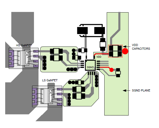
Figure 1. NCP51820 VDD capacitor layout and routing
All traces should be kept as short and straight as possible. Vias can be used because the VDD current is relatively low. The SGND return plane is useful for its shielding properties and keeping all signal side ground loops at the same potential and is recommended. The SGND plane is placed on layer 2, keeping it close to the signal side components and the NCP51820. All signal side components are placed on the SGND plane and connected through vias. A direct connection should be made between the VDD pin and the VDD capacitor, preferably using vias as the return connection to the SGND plane.
As shown in Figure 1, the ground connections of the two VDD capacitors are tied together and connected to the SGND plane through a single via. If possible, it is best to use an uninterrupted solid SGND ground plane to avoid ground loops. It is recommended to extend the “quiet” SGND plane under the NCP51820 to help shield the driver IC from noise. Note in Figure 1 that the SGND plane does not extend under the NCP51820 gate driver output pins. This is intentional to avoid coupling noise from the gate drive di/dt peak source and sink currents into the SGND plane.
VBST Capacitor and Diode, VDDH and VDDL Bypass Capacitors
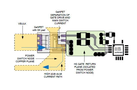
The VBST capacitor should be placed as close to the VBST pin as possible. The VBST capacitor return pin should be connected to the driver SW pin, VDDH return pin, and source Kelvin pin of the GaNFET. Each connection is made through vias to the HS gate return plane as shown in Figure 2. It is important to note that there should be no connection from the power stage switch node back to the NCP51820. Do not connect the VBST capacitor to the power stage switch node. The only connection to the “switch node” is through the HS GaNFET source Kelvin pin.
The HS gate return plane should be designed so that it does not overlap or interact with the power stage switch node. Likewise, the LS gate return plane should be designed so that it does not overlap or interact with the LS GaNFET power ground. Do not place the SGND plane under the VBST diode or VBST capacitor because of the high dV/dt on the cathode of the VBST diode, which may inject noise into the SGND plane.

Figure 2. NCP51820 VBST capacitor and diode, VDDH and VDDL capacitors
The VDDH capacitor should be placed as close to the VDDH pin as possible. The VDDH capacitor return pin should be connected to the HS gate return plane (sharing a double via connection with the VBST capacitor) through vias as shown in Figure 2.
The VDDL capacitor should be placed as close to the VDDL pin as possible. The VDDL capacitor return pin should be connected to the LS gate return plane through vias as shown in Figure 2. The VDDL capacitor return pin must be connected to the PGND pin on the driver. The VDDL capacitor return pin is connected to the LS gate return plane through a via, which is also connected to the driver PGND pin through a via.
Due to the high gate drive current peaks and to reduce via parasitic inductance, multiple vias are required for VBST, VDDH, and VDDL. In this example, four vias are used for each GaNFET gate return connection. This is a reasonable compromise between getting a low impedance connection between the NCP51820 gate driver return pin and the GaNFET return pin, while maintaining a solid return plane and good shielding integrity. If possible, it is better to use conductive filled vias because of their lower associated inductance.
Gate Drive Routing
When the NCP51820 sources current to the HS GaNFET gate, the gate current comes from the charge stored in the VDDH regulator bypass capacitor. As shown in Figure 3, the source current flows through the HO driver source impedance and gate-source resistance into the GaNFET gate. The current then returns from the GaNFET source Kelvin pin and back to the VDDH bypass capacitor.
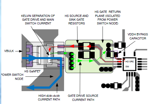
Figure 3. High-side gate drive source current
When the NCP51820 sinks current from the HS GaNFET, the current comes from the energy stored in the gate-source capacitance. As shown in Figure 4, the sink current flows from the HS GaNFET gate, through the gate sink resistor, the HO SINK driver impedance and the SW pin, back to the GaNFET source Kelvin pin.
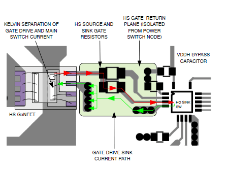
Figure 4. High-side gate drive source current
When the NCP51820 sources current to the LS GaNFET gate, the gate current comes from the charge stored in the VDDL regulator bypass capacitor
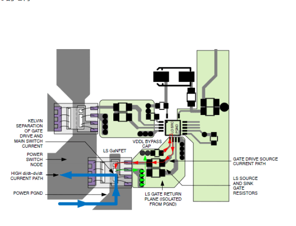
Figure 5. Low-side gate drive source current
When the NCP51820 sinks current from the LS GaNFET, the current comes from the energy stored in the gate-source capacitance. As shown in Figure 6, the sink current flows from the LS GaNFET gate, through the gate sink resistor, the LO SINK driver impedance, and the PGND pin, back to the GaNFET source Kelvin pin.
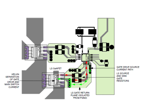
Figure 6. Low-side gate drive sink current
GaNFETs can operate at high switching frequencies, with high dV/dt (100 V/ns and higher) occurring during drain-source switching. GaN has a low gate-source turn-on threshold (<2 V), so the gate drive source and sink paths must be kept as short and direct as possible to mitigate the adverse effects of trace parasitic inductance. Excessive parasitic inductance in the gate loop can cause gate oscillation or high-frequency ringing that exceeds the gate-source threshold voltage. Vias in the gate drive and return paths should only be used when absolutely necessary. It is best to use vias filled with conductive material because each such via has much less inductance. Using a current-carrying return plane under the gate resistor and associated routing to provide a return path directly below the source and sink paths helps reduce loop inductance.
The NCP51820 high-side and low-side drivers are isolated from each other internally. For the high-side, the SW pin must be isolated from the power switch node to prevent switching noise from being injected into the gate drive path, and it can only be connected to the SK pin on the high-side GaNFET. The Kelvin connection between the source Kelvin pin and the power pin is the only electrical connection between the NCP51820 SW pin and the power stage switch node, as shown in Figure 3 and Figure 4. Similarly, the routing of the low-side gate drive should isolate the NCP51820 PGND pin from the power stage PGND and can only be connected to the SK of the low-side GaNFET. The design goal is to avoid the power PGND noise from being injected into the low-side gate drive path. Inside the low-side GaNFET, there is a Kelvin connection between the SK pin and the power pin, which is the actual connection between the NCP51820 PGND and the power PGND, as shown in Figure 5 and Figure 6.
The lengths of the HS and LS gate traces should be as equal as possible within the design allowed. This helps ensure that both GaNFETs have similar gate drive impedance. The staggered alignment of the high-side and low-side GaNFETs has a dual purpose: it allows for nearly symmetrical and equidistant gate drive routing, and it allows for the use of larger, higher current power switch node copper contacts.
It is best to assign the HS and LS return planes to Layer 2 and place them directly below the gate drive resistors and traces, which helps reduce the gate drive loop inductance. For the high-side GaNFET, since the VDDH bypass capacitor return pin and the NCP51820 SW pin are separated by the HO source and HO sink traces, an unfilled via can be used to connect to the source Kelvin pin of the GaNFET through the HS gate return plane. Multiple vias are recommended to help reduce via inductance. Note that the gate drive current path is isolated from the power switch node current path to minimize the injection of noise in the main current path into the gate drive current path.
For the low-side GaNFET, since the VDDL bypass capacitor return pin and the NCP51820 PGND pin are separated by the LO source and LO sink traces, an unfilled via can be used to connect to the source Kelvin pin of the GaNFET through the LS gate return plane. Multiple vias are recommended to help reduce via parasitic inductance. Note that the gate drive current path is isolated from the power PGND current path to minimize the injection of noise in the main current path into the gate drive current path.
Signal Ground (SGND) and Power Ground (PGND)
SGND is the ground for all internal control logic and digital inputs. Internally, the SGND and PGND pins are isolated from each other. PGND is used as the low-side gate drive and return reference.
For half-bridge power topologies or any application using a current sense transformer, the NCP51820 SGND and PGND should be connected together on the PCB. In such applications, it is recommended to connect the SGND and PGND pins together on the PCB with a short low impedance trace and keep them as close to the NCP51820 as possible. The ideal location to make the SGND to PGND connection is right below the NCP51820, as shown in Figure 7.

Figure 7. PGND to SGND, 0 Ω single point connection
For low power applications, such as active clamp flyback or forward converters, a current sense resistor RCS is usually used in the low-side GaN FET source leg. In such applications, the NCP51820 PGND and SGND pins must not be connected on the PCB because RCS will be shorted through this connection. The NCP51820 low-side driver circuit can withstand a common-mode voltage of -3.5 V to +3.5 V. Most current sense voltage signals are less than 1 V, so it is easy for the low side driver stage to “float” above the voltage VRCS generated by the current sense. As shown in Figure 8, the entire low side gate drive floats above VRCS. This is important because it ensures that there is no loss in gate drive amplitude, so the full VDDL voltage appears at the low side GaN FET gate source terminals.
When the circuit is laid out as described above, the controller HO/LO paths connected to the NCP51820 HIN and LIN must be returned to the controller GND to complete the circuit. Therefore, the NCP51820 SGND and controller GND must be connected. This is achieved by connecting the NCP51820 SGND and controller GND to the SGND plane using vias, as shown in Figure 14. The SGND plane is used only for signal and signal side VDD returns, and also acts as a shield for the signal. The VRCS return pin must also be connected to the controller GND, which should be done with a single low impedance trace that should be as close as possible to (or underneath) the VRCS trace. This will connect the power stage PGND to SGND at a single point and isolate the high dV/dt and di/dt on the power stage PGND from the SGND plane.
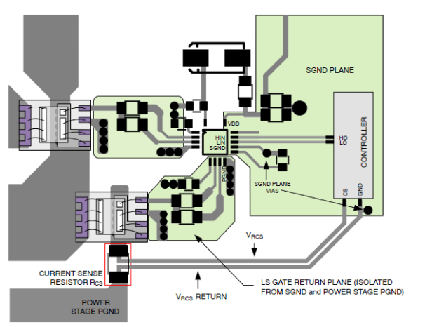
Figure 8. LS gate return isolation and VRCS connection
Switching performance verification
The PCB design techniques presented in this article were used in the layout of a half-bridge power stage driving GaNFETs using the NCP51820.
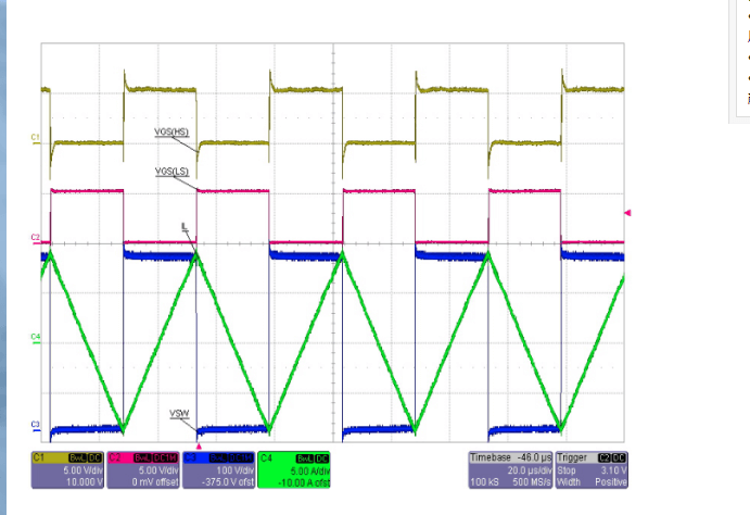
Figure 9. 650 V, 18 A, HEMT, GaNFET, 350 V, 10 APK
Figure 9 shows the steady-state waveforms driving two 650 V, 18 A, 90 mΩ GaNFETs. Channel 1 (yellow) is the high-side gate-source voltage, Channel 2 (red) is the low-side gate-source voltage, Channel 3 (blue) is the switch node voltage (low-side GaN VDS), and Channel 4 (green) is the inductor current. The high-side gate-source voltage (Channel 1, yellow) shows slight overshoot and undershoot, which is a byproduct of using a high-voltage probe to measure a low-voltage floating signal (measured between the gate and the power switch node). Channel 2 (red) shows a “more realistic” measurement of the gate-source voltage, where the low-side GaNFET gate-source voltage is measured between the gate and PGND. It can be seen that the gate drive edges are very sharp and clean. Likewise, the switch node voltage (Channel 3, blue) has no ringing, overshoot, or undershoot.
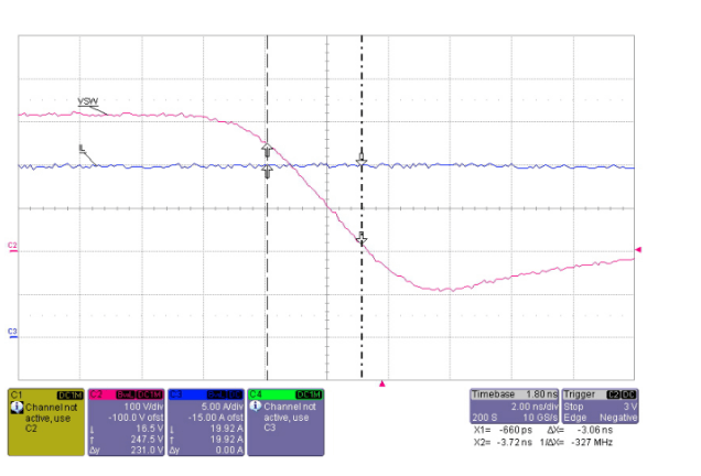
Figure 10. 600 V, 26 A, HEMT, GIT, GaNFET, dV/dt = 75 V/ns, 320 V, 20 APK
The waveforms shown in Figure 10 are the result of driving two HEMT, GIT, 600 V, 26 A, 56 mΩ GaNFETs with higher current capability than the devices used in Figure 9. To achieve high dV/dt, a significant drain current ID is required. For example, the measurements shown were taken at ID = 20 , resulting in a measured VDS dV/dt = 75 V/ns. The triangular peak inductor current appears pure DC due to the time base (2 ns/div) required to make this measurement. The 100 V undershoot of the VSW waveform is a result of the measurement technique used to display the high dV/dt and does not really exist at the switch node.
Successfully utilizing wide bandgap semiconductors in high voltage, high frequency PCB design requires a better understanding of the negative effects of parasitic inductance and capacitance. A thorough understanding of the importance of electrical return planes, shielding, galvanic separation, isolation, and careful routing are essential to fully realize the performance benefits of GaN technology. This article highlights the important PCB design guidelines that must be employed to achieve a successful design when driving GaN power switches used in high speed power topologies using the NCP51820. These techniques have been validated using measured waveforms to achieve excellent results.