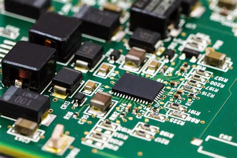
Several misunderstandings about differential signal layout on PCB
Misunderstanding 1
It is believed that differential signals do not need a ground plane as a return path, or that differential traces provide return paths for each other. The reason for this misunderstanding is that people are confused by surface phenomena or do not have a deep enough understanding of the mechanism of high-speed signal transmission.
Although differential circuits are insensitive to noise signals such as ground bounce and other noise signals that may exist on the power supply and ground planes.
The partial return offset of the ground plane does not mean that the differential circuit does not use the reference plane as the signal return path. In fact, in signal return analysis, the mechanism of differential traces and ordinary single-ended traces is the same, that is, high-frequency signals always return along the loop with the smallest inductance. The biggest difference is that in addition to coupling to the ground, differential lines also have mutual coupling. The one with stronger coupling becomes the main return path.
In PCB circuit design, the coupling between differential traces is generally small, often accounting for only 10~20% of the coupling degree, and more is coupling to the ground, so the main return path of differential traces still exists on the ground plane.
When the ground plane is discontinuous, the coupling between the differential traces in the area without the reference plane will provide the main return path
Although the discontinuity of the reference plane does not have a serious impact on the differential traces as on the ordinary single-ended traces, it will still reduce the quality of the differential signal and increase EMI, so it should be avoided as much as possible.
Some designers also believe that the reference plane under the differential traces can be removed to suppress some common-mode signals in differential transmission, but theoretically this approach is not advisable. How to control the impedance? Not providing a ground impedance loop for the common-mode signal will inevitably cause EMI radiation, which is more harmful than beneficial.
Therefore, the return path of the PCB ground layer should be kept wide and short. Try not to cross the island (cross the separation area of the adjacent power supply or ground layer.) For example, it is best not to cross the island for USB, SATA and PCI-EXPRESS in the motherboard design. Ensure that there is a complete ground plane or power plane under these signals.
Misunderstanding 2
It is believed that maintaining equal spacing is more important than matching line length. In actual PCB wiring, the requirements of differential design cannot often be met at the same time. Due to factors such as pin distribution, vias, and routing space, proper winding is necessary to achieve the purpose of line length matching, but the result is that some areas of the differential pair cannot be parallel. In fact, the impact of unequal spacing is minimal. In comparison, the impact of line length mismatch on timing is much greater.
From a theoretical analysis, although inconsistent spacing will cause changes in differential impedance,
because the coupling between differential pairs is not significant, the impedance change range is also very small, usually within 10%, which is only equivalent to the reflection caused by a via, which will not have a significant impact on signal transmission. Once the line length is mismatched, in addition to the timing offset, it also introduces common mode components into the differential signal, reducing the signal quality and increasing EMI.
It can be said that the most important rule in the design of PCB differential routing is to match the line length, and other rules can be flexibly handled according to design requirements and actual applications. At the same time, in order to compensate for the impedance matching, a matching resistor can be added between the differential line pairs at the receiving end. Its value should be equal to the value of the differential impedance. In this way, the signal quality will be better.

Therefore, the following two points are recommended:
(A) Use terminal resistors to achieve maximum matching of differential transmission lines. The resistance is generally between 90 and 130Ω. The system also needs this terminal resistor to generate a normal differential voltage;
(B) It is best to use a surface mount resistor with an accuracy of 1 to 2% to bridge the differential line. If necessary, two resistors with a resistance of 50Ω each can be used and grounded through a capacitor in the middle to filter out common mode noise.
Usually, the matching requirements for the CLOCK and other requirements of differential signals are within +/-10mils.
Misconception 3
It is believed that differential traces must be very close. Bringing differential traces close together is nothing more than to enhance their coupling, which can not only improve immunity to noise, but also make full use of the opposite polarity of the magnetic field to offset the electromagnetic interference to the outside world. Although this approach is very beneficial in most cases, it is not absolute.
If we can ensure that they are fully shielded and not interfered with by the outside world, then we don’t need to achieve the purpose of anti-interference and EMI suppression through strong coupling with each other. How can we ensure that the differential traces have good isolation and shielding? Increasing the spacing between other signal traces is one of the most basic ways.
The electromagnetic field energy decreases with the square of the distance.
Generally, when the line spacing exceeds 4 times the line width, the interference between them is extremely weak and can be basically ignored. In addition, the isolation of the ground plane can also play a good shielding role. This structure is often used in high-frequency (above 10G) IC package PCB design. It is called CPW structure, which can ensure strict differential impedance control (2Z0).
Differential traces can also be routed in different signal layers, but this method is generally not recommended because the differences in impedance and vias generated by different layers will destroy the effect of differential mode transmission and introduce common mode noise. In addition, if the coupling between two adjacent layers is not tight enough, the ability of the differential trace to resist noise will be reduced, but if the appropriate spacing with the surrounding traces can be maintained, crosstalk will not be a problem. At normal frequencies (below GHz), EMI will not be a serious problem. Experiments have shown that for differential lines 500 Mils apart, the radiation energy attenuation at 3 meters away has reached 60 dB, which is enough to meet the FCC’s electromagnetic radiation standards. Therefore, designers do not need to worry too much about electromagnetic incompatibility problems caused by insufficient differential line coupling.


