Single-Sided Printed Circuit Boards (PCBs): An Overview
Introduction
Printed Circuit Boards (PCBs) are the backbone of modern electronics, serving as the foundation upon which electronic components are mounted and interconnected. Among the various types of PCBs, single-sided PCBs are the simplest and most cost-effective option. They are widely used in a variety of applications, from consumer electronics to industrial control systems. This article provides an in-depth look at single-sided PCBs, covering their design, manufacturing process, advantages, limitations, and common applications.
What is a Single-Sided PCB?
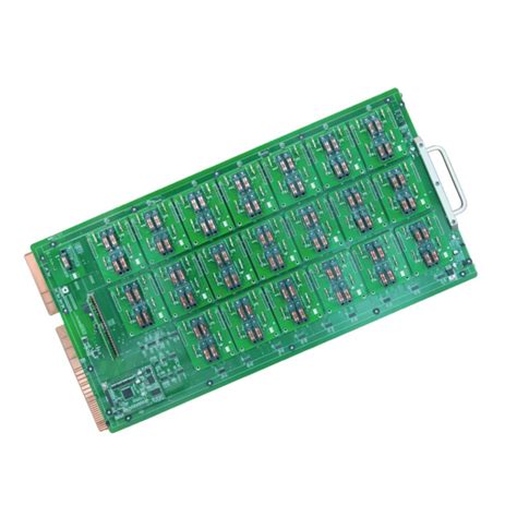
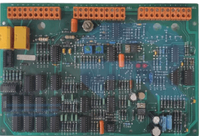
A single-sided PCB, also known as a single-layer PCB, is a type of circuit board that has conductive traces and pads on only one side of the board. The other side is typically left bare or covered with a solder mask to protect the board from environmental factors. Single-sided PCBs are the most basic form of PCBs and are often used in simple electronic devices where the circuit design is not overly complex.
Design Considerations for Single-Sided PCBs
Designing a single-sided PCB requires careful consideration of several factors to ensure optimal performance and manufacturability. Some of the key design considerations include:
- Component Placement: Since all the components and traces are on one side of the board, it is crucial to place components in a way that minimizes the need for complex routing. Components should be arranged to allow for short, direct traces, which can help reduce signal interference and improve the overall performance of the circuit.
- Trace Routing: Trace routing on a single-sided PCB can be challenging due to the limited space available. Designers must carefully plan the layout to avoid crossing traces, which would require the use of jumpers or wire bridges. Proper spacing between traces is also essential to prevent electrical interference and ensure reliable operation.
- Power and Ground Planes: In single-sided PCBs, power and ground connections are typically routed using traces rather than dedicated planes. This can lead to increased resistance and potential voltage drops, especially in high-current applications. Designers must ensure that power and ground traces are sufficiently wide to handle the required current without excessive voltage drop.
- Thermal Management: Since single-sided PCBs have only one layer of conductive material, they may have limited thermal dissipation capabilities. Designers must consider the thermal characteristics of the components and the board itself to prevent overheating. This may involve the use of heat sinks, thermal vias, or other cooling solutions.
- Manufacturing Constraints: Single-sided PCBs are subject to certain manufacturing constraints, such as minimum trace width, spacing, and hole size. Designers must adhere to these constraints to ensure that the board can be reliably manufactured.
Manufacturing Process of Single-Sided PCBs
The manufacturing process for single-sided PCBs involves several steps, each of which must be carefully controlled to ensure the quality and reliability of the final product. The typical manufacturing process includes the following steps:
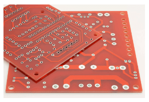
- Substrate Preparation: The process begins with the preparation of the substrate, which is typically made of a non-conductive material such as fiberglass (FR-4). The substrate is cut to the desired size and shape, and any necessary holes or cutouts are drilled.
- Copper Cladding: A thin layer of copper is laminated onto one side of the substrate. This copper layer will form the conductive traces and pads of the PCB.
- Photoresist Application: A photoresist material is applied to the copper-clad substrate. The photoresist is a light-sensitive material that will harden when exposed to ultraviolet (UV) light.
- Exposure and Development: A photomask, which contains the circuit pattern, is placed over the photoresist-coated substrate. The assembly is then exposed to UV light, which hardens the photoresist in the areas corresponding to the circuit pattern. The unexposed photoresist is then removed using a developer solution, leaving behind the desired circuit pattern.
- Etching: The exposed copper is etched away using a chemical solution, leaving only the copper traces and pads that form the circuit. The remaining photoresist is then stripped away, revealing the final circuit pattern.
- Solder Mask Application: A solder mask is applied to the board to protect the copper traces from oxidation and to prevent solder bridges during component assembly. The solder mask is typically green, but other colors are also available.
- Silkscreen Printing: A silkscreen layer is printed onto the board to add component labels, logos, and other identifying marks. This layer is typically white, but other colors can be used.
- Surface Finish: A surface finish is applied to the exposed copper pads to protect them from oxidation and to improve solderability. Common surface finishes include HASL (Hot Air Solder Leveling), ENIG (Electroless Nickel Immersion Gold), and OSP (Organic Solderability Preservative).
- Electrical Testing: The finished PCB is subjected to electrical testing to ensure that all connections are correct and that there are no short circuits or open circuits.
- Final Inspection and Packaging: The PCB is inspected for any visual defects, such as scratches or misaligned components. Once the inspection is complete, the boards are packaged and shipped to the customer.
Advantages of Single-Sided PCBs
Single-sided PCBs offer several advantages that make them a popular choice for many applications:
- Cost-Effective: Single-sided PCBs are the most cost-effective type of PCB due to their simple design and manufacturing process. They require fewer materials and less complex equipment, which translates to lower production costs.
- Ease of Design: The simplicity of single-sided PCBs makes them easier to design compared to multi-layer boards. This is particularly beneficial for simple circuits or for designers who are new to PCB design.
- Quick Turnaround: The manufacturing process for single-sided PCBs is relatively quick, which can lead to faster turnaround times for prototypes and small production runs.
- Reliability: Single-sided PCBs are generally more reliable than more complex multi-layer boards because there are fewer potential points of failure. The simplicity of the design reduces the likelihood of manufacturing defects.
- Ease of Repair: In the event of a fault, single-sided PCBs are easier to repair because all the components and traces are accessible from one side of the board.
Limitations of Single-Sided PCBs
Despite their advantages, single-sided PCBs also have some limitations that may make them unsuitable for certain applications:
- Limited Complexity: Single-sided PCBs are not suitable for complex circuits that require a high density of components and interconnections. The limited space on one side of the board can make it difficult to route all the necessary traces without crossing, which would require the use of jumpers.
- Signal Integrity Issues: In high-frequency or high-speed applications, single-sided PCBs may suffer from signal integrity issues due to the lack of a ground plane. This can lead to increased electromagnetic interference (EMI) and crosstalk between traces.
- Thermal Management: Single-sided PCBs have limited thermal dissipation capabilities, which can be a concern in high-power applications. The lack of additional layers for heat dissipation can lead to overheating and reduced reliability.
- Size Constraints: The limited space on a single-sided PCB can make it difficult to design compact circuits. This can be a disadvantage in applications where space is at a premium.
Common Applications of Single-Sided PCBs
Single-sided PCBs are used in a wide range of applications, particularly in devices where the circuit design is relatively simple and cost is a primary concern. Some common applications include:
- Consumer Electronics: Single-sided PCBs are commonly used in consumer electronics such as calculators, remote controls, and simple audio devices. These devices typically have straightforward circuit designs that do not require the complexity of multi-layer boards.
- Power Supplies: Single-sided PCBs are often used in power supplies and battery chargers, where the circuit design is relatively simple and the primary concern is cost-effectiveness.
- LED Lighting: Single-sided PCBs are widely used in LED lighting applications, such as LED strips and light bulbs. The simplicity of the circuit design and the low cost of single-sided PCBs make them an ideal choice for these applications.
- Industrial Control Systems: Single-sided PCBs are used in various industrial control systems, such as relays, timers, and sensors. These applications often require reliable and cost-effective solutions, which single-sided PCBs can provide.
- Automotive Electronics: Single-sided PCBs are used in various automotive electronics, such as dashboard controls, lighting systems, and simple sensors. The ruggedness and reliability of single-sided PCBs make them suitable for the harsh environments found in automotive applications.
Conclusion
Single-sided PCBs are a fundamental component of modern electronics, offering a cost-effective and reliable solution for a wide range of applications. While they may not be suitable for highly complex or high-speed circuits, their simplicity, ease of design, and quick turnaround times make them an attractive option for many designers and manufacturers. As technology continues to evolve, single-sided PCBs will likely remain a key player in the electronics industry, particularly in applications where cost and simplicity are paramount.


