Single-Sided vs Double-sided PCBs: Key Differences and Applications
Introduction to PCB Basics
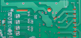
Printed Circuit Boards (PCBs) form the foundation of nearly all modern electronic devices, from simple calculators to sophisticated supercomputers. These boards provide the mechanical structure to mount electronic components and the electrical connections between them through conductive pathways etched from copper sheets. Among the various types of PCBs available, single-sided and double-sided configurations represent the most fundamental designs, each with distinct characteristics that make them suitable for different applications.
Understanding the differences between single-sided and double-sided PCBs is essential for electronics designers, engineers, and manufacturers. The choice between these two types affects not only the circuit’s functionality but also its cost, size, complexity, and manufacturing process. This article provides a comprehensive comparison of these two fundamental PCB types, examining their structures, manufacturing processes, advantages, limitations, and typical applications.
Structural Differences
Single-sided PCB Construction
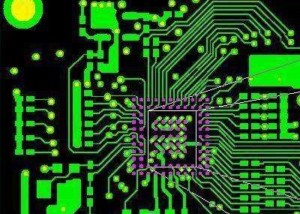
Single-sided PCBs represent the simplest form of printed circuit boards. As the name suggests, these boards have conductive copper traces on only one side of the substrate material, typically fiberglass-reinforced epoxy (FR-4). The structure consists of:
- Base Substrate: The non-conductive core material (usually FR-4) that provides mechanical support
- Copper Layer: A thin layer of copper foil laminated to one side of the substrate
- Solder Mask: A protective layer applied over the copper traces to prevent oxidation and accidental shorts
- Silkscreen: The top layer that displays component labels, logos, and other identifying marks
All electronic components are mounted on the opposite side from the copper traces, with their leads passing through holes (for through-hole components) or placed directly on pads (for surface-mount devices) to connect with the copper pathways.
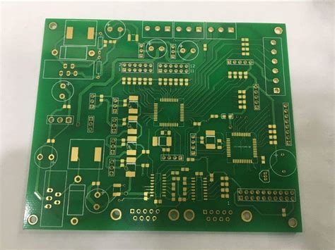
Double-sided PCB Construction
Double-sided PCBs feature conductive copper layers on both sides of the substrate, effectively doubling the available area for routing traces. The structure includes:
- Base Substrate: The central insulating core (typically FR-4)
- Copper Layers: Copper foil laminated to both sides of the substrate
- Through-holes or Vias: Plated holes that electrically connect the two copper layers
- Solder Mask: Protective coating applied to both sides
- Silkscreen: Printing on one or both sides for component identification
The presence of conductive layers on both sides allows for more complex circuit designs and higher component density. Components can be mounted on either or both sides of the board, depending on the design requirements.
Manufacturing Process Comparison
Single-sided PCB Fabrication
The manufacturing process for single-sided PCBs is relatively straightforward:
- Substrate Preparation: The base material is cut to the required size
- Copper Lamination: Copper foil is bonded to one side of the substrate
- Drilling: Holes for component leads are drilled
- Patterning: The circuit pattern is transferred to the copper layer using photolithography or screen printing
- Etching: Unwanted copper is removed using chemical etchants, leaving only the desired traces
- Solder Mask Application: A protective coating is applied over the copper traces
- Silkscreen Printing: Component identifiers and other markings are added
- Surface Finishing: Exposed copper areas may receive coatings like HASL (Hot Air Solder Leveling) or ENIG (Electroless Nickel Immersion Gold)
- Testing: Basic electrical tests verify circuit continuity
The simplicity of this process contributes to lower production costs and faster turnaround times compared to double-sided boards.
Double-sided PCB Fabrication
Double-sided PCB manufacturing involves additional steps to create connections between the two copper layers:
- Substrate Preparation: Base material is prepared as with single-sided boards
- Double-sided Copper Lamination: Copper foil is bonded to both sides of the substrate
- Drilling: Holes are drilled for through-hole components and vias
- Plating Through Holes: The holes are electroplated to create conductive paths between layers
- Patterning: Circuit patterns are transferred to both sides, often using more precise photolithography
- Etching: Unwanted copper is removed from both sides simultaneously
- Solder Mask Application: Protective coating applied to both sides
- Silkscreen Printing: Markings added to one or both sides
- Surface Finishing: Both sides receive protective coatings
- Testing: More comprehensive testing including continuity between layers
The additional plating process and more complex patterning requirements make double-sided PCB fabrication more time-consuming and expensive than single-sided production.
Electrical Performance Differences
Current Carrying Capacity
For a given trace width, single-sided PCBs typically have slightly better current carrying capacity because:
- The copper thickness is often slightly greater on single-sided boards (typically 1 oz/ft² compared to 0.5-1 oz/ft² per side for double-sided)
- No vias or plated through-holes are needed, eliminating potential points of resistance
However, double-sided boards can achieve higher overall current capacity by using both layers in parallel for power distribution.
Signal Integrity and Crosstalk
Double-sided PCBs offer significant advantages for signal integrity:
- Ground Planes: One side can be used as a continuous ground plane, reducing noise and improving signal quality
- Shielding: Sensitive traces can be routed on one side with a ground plane on the opposite side for shielding
- Reduced Crosstalk: Proper use of both layers allows for better separation of high-speed signals
Single-sided boards are more susceptible to crosstalk and noise because all traces must share the same layer, making proper spacing and routing more challenging.
High-frequency Performance
For high-frequency applications, double-sided PCBs are vastly superior:
- Controlled impedance traces can be implemented using the ground plane as a reference
- Shorter return paths reduce inductance and electromagnetic interference (EMI)
- Better heat dissipation through vias and the second copper layer
Single-sided boards are generally unsuitable for high-frequency designs due to their poor impedance control and longer return paths.
Design Considerations and Limitations
Component Density and Routing
Single-sided PCBs face significant limitations in component density and routing:
- All connections must be made without crossing traces on the same layer
- Complex circuits may require jumper wires to bypass these limitations
- Component placement is constrained by routing requirements
Double-sided PCBs overcome these limitations:
- Traces can cross between layers using vias
- Components can be placed on both sides of the board
- Higher component density is achievable
- More efficient use of board space
Thermal Management
Double-sided PCBs offer better thermal performance:
- The additional copper layer helps dissipate heat
- Thermal vias can transfer heat between layers
- Components can be spaced further apart to reduce thermal interference
Single-sided boards have poorer thermal characteristics, which can limit power handling capabilities and component lifetime in high-temperature applications.
Design Complexity and Cost
While single-sided PCBs are simpler to design, their limitations often lead to larger board sizes for complex circuits. Double-sided PCBs allow for more compact designs but require:
- More sophisticated design software to manage two layers
- Careful planning of via placement and layer transitions
- Attention to thermal and electrical interactions between layers
The manufacturing cost difference between single and double-sided PCBs has narrowed in recent years, making double-sided boards increasingly attractive even for relatively simple designs.
Applications and Use Cases
Typical Single-sided PCB Applications
Single-sided PCBs are commonly found in:
- Simple consumer electronics (calculators, basic toys)
- Power supplies and LED lighting
- Relays and electromechanical controls
- Automotive applications (non-critical systems)
- Basic sensor modules
- Low-cost electronic appliances
These applications typically feature:
- Low component counts (typically <50 components)
- Low frequency operation (<10MHz)
- Minimal interconnection requirements
- Cost sensitivity that outweighs space constraints
Typical Double-sided PCB Applications
Double-sided PCBs are used in:
- Industrial controls and automation systems
- Power converters and inverters
- Automotive electronics (engine controls, infotainment)
- Medical devices (monitoring equipment)
- Telecommunications equipment
- Computer peripherals
These applications generally require:
- Moderate to high component density
- Better signal integrity than single-sided boards can provide
- Some high-speed signals (up to several hundred MHz)
- More complex power distribution needs
Cost Analysis and Economic Considerations
Material Costs
The raw material cost difference between single and double-sided PCBs is relatively small:
- The additional copper layer represents a minor cost increase
- The substrate material cost is identical
- Solder mask and silkscreen costs are slightly higher for double-sided boards
Manufacturing Costs
The production cost differential is more significant:
- Double-sided boards require additional processing steps (plating, double-sided patterning)
- Alignment between layers adds complexity
- Testing is more involved
- Yield rates may be slightly lower
However, for medium to high volume production, the cost difference per unit becomes less significant.
Total System Cost Considerations
When evaluating total system costs:
- Single-sided designs may require larger boards or additional connectors for jumpers
- Double-sided designs can reduce overall product size, affecting enclosure costs
- Assembly costs may favor double-sided boards due to better component placement options
- Reliability improvements with double-sided boards can reduce warranty costs
For many applications, the total cost advantage of single-sided boards is smaller than the raw PCB cost comparison might suggest.
Future Trends and Technological Developments
The Evolving Role of Single-sided PCBs
While single-sided PCBs are becoming less common in sophisticated electronics, they continue to play important roles:
- Ultra-low-cost applications where every cent matters
- Extremely high-volume consumer products
- Educational kits and prototyping for beginners
- Applications where simplicity is more valuable than miniaturization
Advancements in Double-sided PCB Technology
Double-sided PCB technology continues to evolve:
- Improved via filling techniques for better reliability
- Advanced surface finishes for enhanced solderability
- Thinner materials enabling more flexible applications
- Better thermal management features
The Impact of Multi-layer Alternatives
For many advanced applications, four or more layer PCBs are becoming standard. However, between single and double-sided options:
- Double-sided remains the sweet spot for moderate complexity
- The cost jump to 4-layer is much larger than from single to double-sided
- Many designs can be optimized to stay on two layers rather than moving to four
Conclusion: Choosing Between Single and Double-sided PCBs
The choice between single and double-sided PCBs depends on multiple factors:
- Circuit Complexity: Simple circuits with few components and no crossing traces can use single-sided; more complex designs need double-sided
- Performance Requirements: High-frequency, high-reliability, or noise-sensitive applications favor double-sided
- Space Constraints: Compact designs typically require double-sided layouts
- Cost Sensitivity: For extremely cost-sensitive, high-volume products, single-sided may be preferred
- Thermal Considerations: Power applications often benefit from double-sided thermal management
- Production Volume: The per-unit cost difference shrinks with higher volumes
While single-sided PCBs maintain their place in simple, cost-driven applications, double-sided PCBs offer significantly greater design flexibility and performance capabilities for only a modest cost increase. For most modern electronic products beyond the most basic, double-sided PCBs represent the optimal balance of cost, performance, and design freedom.
As PCB manufacturing technology continues to advance, the practical differences between these two fundamental board types may evolve, but their core characteristics and appropriate applications will likely remain distinct for the foreseeable future. Designers must carefully evaluate their specific requirements to make the optimal choice between single and double-sided implementations.