Six Tips to Transfer PCB Schematics to Layout
Six things to consider when transferring PCB schematics to layout. All examples mentioned were developed using the Multisim design environment, but the same concepts apply when using different EDA tools!

Initial Schematic Transfer
The process of transferring the schematic to the layout environment through the netlist file also transfers the device information, netlist, layout information and initial trace width settings.
Here are some recommended steps to prepare for the layout design stage:
- Set the grid and units to appropriate values. For more precise placement control of components and traces, the device grid, copper grid, via grid and SMD grid can be designed to 1mil.
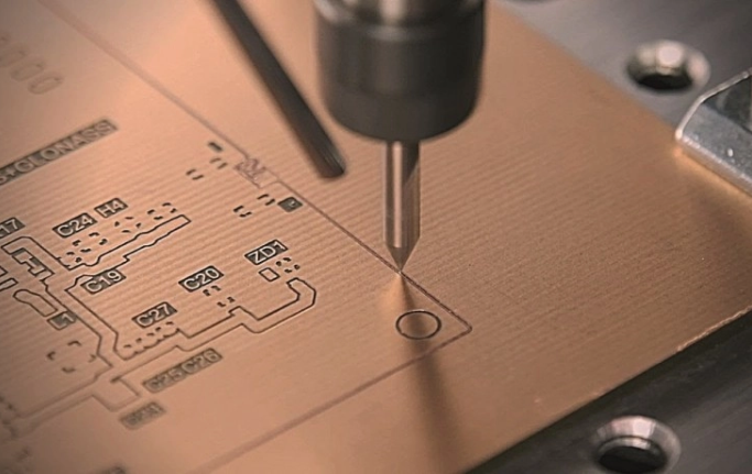
- Set the board frame blank area and vias to the required values. The PCB manufacturer may have specific minimum values or nominal recommended values for blind and buried via settings.
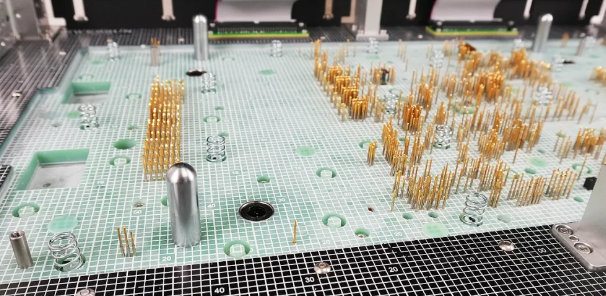
- Set the appropriate pad/via parameters according to the PCB manufacturer’s capabilities. Most PCB manufacturers can support smaller vias with a drill diameter of 10mil and a pad diameter of 20mil.
- Set up design rules as required.
- Set up custom shortcuts for commonly used layers so that you can quickly switch layers (and create vias) when routing.
Handling Errors During Schematic Transfer
A common error during schematic transfer is non-existent or incorrect footprint assignments. It is important to note that:
If there is a device in the schematic without a footprint, a warning message will pop up indicating that the virtual component cannot be exported. In this case, no default footprint information will be passed to the layout and the component will simply be deleted from the layout.
If the footprint is passed, but does not correctly match a valid footprint shape, a warning message indicating a mismatch will also be generated during the transfer process.
Correct the footprint assignment in the schematic, or create a valid footprint for any device. After correction, perform the forward annotation step to update and synchronize the design information.
Updating the design through annotation
Annotation is the process of transferring design changes from schematic to layout or from layout to schematic. Backward annotation (layout to schematic) and forward annotation (schematic to layout) are key to keeping designs accurate.
To protect the work that has already been done, back up and archive the current versions of the schematic and layout files before any major forward or back annotation steps.
Do not attempt to make changes in both the schematic and layout at the same time. Make changes to only one part of the design (either the schematic or the layout), then perform the correct annotation steps to synchronize the design data.
Renumbering Components
Component renumbering is a function that renumbers the components on the PCB into a specific sequence. Reference designators should be ordered from top to bottom and from left to right on the PCB. This makes it easier to locate the component on the board during assembly, test, and troubleshooting.
Handling Last-Minute Component or Netlist Changes
Last-minute PCB component or netlist changes are undesirable, but sometimes they have to be made because of component availability issues or the detection of last-minute design errors. If the component or netlist needs to be changed, it should be done in the schematic and then forward-annotated to the layout tool. Here are some tips:
- If you add a new device after layout design has begun (such as adding a pull-up resistor to an open-drain output), add the resistor and network to the design from the schematic. After forward annotation, the resistor will be displayed outside the board outline as an unplaced component, and the flying wires will be displayed to indicate the connection network. Next, move the component inside the board outline and perform normal routing.
- Backward annotation works well with reference number changes, such as post-layout renumbering.
Locating devices through highlight selection
One way to browse specific components or traces in the schematic during PCB layout is to use the ‘Highlight Selection’ feature. This feature allows you to select a component or a trace (or multiple objects) and then see where they are located in the schematic.
This feature is especially useful when matching bypass capacitors and their corresponding IC connections. Conversely, it is also possible to locate specific components or traces in the layout while browsing the schematic.