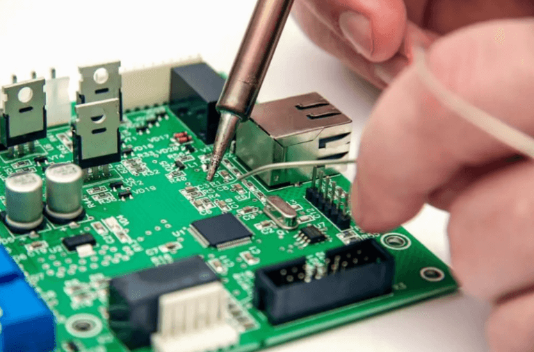
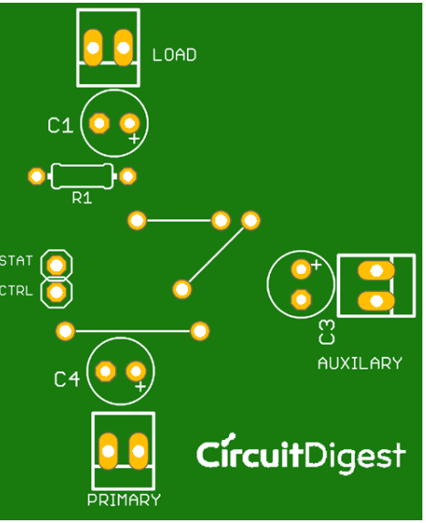
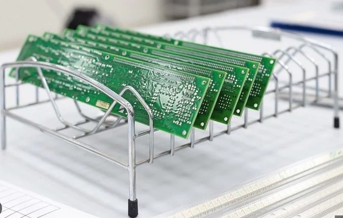
Small batch pcb
Benefits Of Small Batch PCB Prototyping
Small batch PCB prototyping offers numerous advantages that can significantly enhance the development process for electronic products.
One of the primary benefits is the ability to test and validate designs before committing to large-scale production.
By creating a limited number of printed circuit boards, engineers and designers can identify and rectify any potential issues early in the development cycle. This iterative process not only saves time but also reduces the risk of costly errors that could arise during mass production.
Moreover, small batch PCB prototyping provides a cost-effective solution for startups and small businesses.
Large-scale production often requires substantial financial investment, which can be prohibitive for companies with limited resources. By opting for small batch production, these entities can manage their budgets more effectively while still achieving high-quality results. This approach allows for the allocation of funds to other critical areas such as research and development, marketing, and customer acquisition.
In addition to cost savings, small batch PCB prototyping offers greater flexibility in design modifications.
As the market demands and technological advancements evolve, the ability to quickly adapt and refine product designs becomes crucial. Small batch production enables rapid iterations, allowing designers to incorporate feedback and make necessary adjustments without significant delays. This agility is particularly beneficial in industries where innovation and time-to-market are key competitive factors.
Furthermore, small batch PCB prototyping facilitates better communication and collaboration among team members.
With a tangible prototype in hand, engineers, designers, and stakeholders can engage in more productive discussions and brainstorming sessions. This hands-on approach fosters a deeper understanding of the product’s functionality and performance, leading to more informed decision-making. Additionally, having a physical prototype can aid in securing investment or gaining customer interest, as it provides a concrete representation of the concept.
Another notable advantage of small batch PCB prototyping is the opportunity for thorough testing and quality assurance.
By producing a limited number of units, companies can conduct comprehensive evaluations to ensure that the product meets all necessary standards and specifications. This rigorous testing phase helps identify any potential flaws or weaknesses, allowing for corrective measures to be implemented before full-scale production. Consequently, this proactive approach enhances the overall reliability and performance of the final product.
Moreover, small batch PCB prototyping supports environmental sustainability.
Large-scale production often results in significant waste and resource consumption. In contrast, small batch production minimizes material usage and reduces the environmental footprint. By adopting this approach, companies can contribute to a more sustainable manufacturing process, aligning with global efforts to reduce waste and promote eco-friendly practices.
In conclusion, small batch PCB prototyping offers a multitude of benefits that can greatly impact the development and success of electronic products. From cost savings and design flexibility to improved communication and rigorous testing, this approach provides a strategic advantage for companies of all sizes. By embracing small batch production, businesses can navigate the complexities of product development with greater efficiency and confidence, ultimately delivering high-quality, innovative solutions to the market.
Cost-Effective Strategies For Small Batch PCB Production
In the realm of electronics manufacturing, small batch PCB (Printed Circuit Board) production has become increasingly significant. This trend is driven by the need for rapid prototyping, custom designs, and the flexibility to adapt to evolving technological demands. However, producing PCBs in small quantities can be cost-prohibitive if not approached with strategic planning. Therefore, understanding cost-effective strategies for small batch PCB production is essential for businesses and hobbyists alike.
To begin with, one of the most effective strategies is to optimize the design phase.
By meticulously planning the PCB layout and minimizing errors, manufacturers can reduce the need for costly revisions. Utilizing design software that offers simulation and validation tools can help identify potential issues before the production process begins. This proactive approach not only saves time but also reduces material wastage, thereby lowering overall costs.
Another crucial aspect is the selection of materials. While it might be tempting to opt for the highest quality materials available, it is important to balance quality with cost.
For small batch production, choosing materials that meet the necessary specifications without exceeding them can result in significant savings. Additionally, sourcing materials from reliable suppliers who offer competitive pricing can further reduce expenses.
Furthermore, leveraging economies of scale, even in small batch production, can be beneficial.
By consolidating orders or collaborating with other small-scale manufacturers, it is possible to achieve bulk pricing on materials and components. This collaborative approach can also extend to sharing production facilities or equipment, thereby spreading the fixed costs over multiple projects and reducing the per-unit cost.
In addition to material and design considerations, the choice of manufacturing process plays a pivotal role in cost management.
Traditional manufacturing methods, such as photolithography, can be expensive for small batches due to the setup costs involved. However, modern techniques like additive manufacturing or 3D printing offer a more cost-effective alternative. These methods allow for rapid prototyping and small-scale production without the need for extensive setup, making them ideal for small batch PCB production.
Moreover, outsourcing production to specialized PCB manufacturers can also be a cost-effective strategy.
These manufacturers often have the expertise and equipment to produce high-quality PCBs at a lower cost than in-house production. By outsourcing, businesses can take advantage of the manufacturer’s economies of scale, advanced technology, and skilled workforce, all of which contribute to cost savings.
Additionally, implementing a just-in-time (JIT) production approach can help manage costs effectively.
By producing PCBs only when they are needed, businesses can avoid the costs associated with excess inventory and storage. This approach also allows for greater flexibility in responding to changes in demand or design modifications, further enhancing cost efficiency.
Lastly, continuous improvement and feedback loops are essential for maintaining cost-effectiveness in small batch PCB production.
By regularly reviewing production processes, identifying inefficiencies, and implementing improvements, businesses can ensure that they remain competitive and cost-effective. Engaging with customers and gathering feedback can also provide valuable insights into areas for improvement and innovation.
In conclusion, small batch PCB production presents unique challenges, but with strategic planning and the implementation of cost-effective strategies, it is possible to achieve high-quality results without incurring prohibitive costs. By optimizing design, selecting appropriate materials, leveraging economies of scale, choosing the right manufacturing process, outsourcing when necessary, adopting just-in-time production, and continuously improving processes, businesses can navigate the complexities of small batch PCB production efficiently and economically.
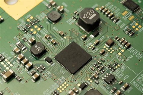
Quality Control Techniques In Small Batch PCB Manufacturing
In the realm of small batch PCB (Printed Circuit Board) manufacturing, quality control is paramount to ensure the reliability and functionality of the final product. Given the limited quantity of units produced, each board must meet stringent standards to avoid costly errors and rework. Various quality control techniques are employed throughout the manufacturing process to achieve this objective, starting from the initial design phase and extending through to the final inspection.
To begin with, the design phase is critical in setting the foundation for quality control.
Design for Manufacturability (DFM) principles are applied to ensure that the PCB layout is optimized for production. This involves checking for common design errors such as incorrect pad sizes, trace widths, and spacing issues. Advanced software tools are often utilized to perform Design Rule Checks (DRC) and Electrical Rule Checks (ERC), which help identify potential issues before the manufacturing process begins. By addressing these issues early, manufacturers can significantly reduce the likelihood of defects in the final product.
Once the design is finalized, the focus shifts to the fabrication process.
During this stage, several quality control techniques are employed to ensure that the physical board meets the required specifications. One such technique is Automated Optical Inspection (AOI), which uses high-resolution cameras to capture images of the PCB and compare them against the design files. This allows for the detection of defects such as missing components, solder bridges, and misalignments. AOI is particularly useful in small batch production, where manual inspection may not be feasible due to time constraints.
In addition to AOI, X-ray inspection is another valuable tool in the quality control arsenal.
This technique is especially useful for detecting hidden defects in multilayer PCBs and components with Ball Grid Array (BGA) packages. By providing a detailed view of the internal structure of the board, X-ray inspection can identify issues such as voids in solder joints, misaligned layers, and internal shorts. This level of scrutiny is essential in small batch manufacturing, where even a single defective board can have significant repercussions.
Moving on to the assembly process, quality control continues to play a crucial role.
Surface Mount Technology (SMT) assembly lines often incorporate solder paste inspection (SPI) systems to ensure that the correct amount of solder paste is applied to each pad. This is followed by another round of AOI to verify the placement and orientation of components before the reflow soldering process. By catching errors at this stage, manufacturers can prevent defects from propagating further down the line.
Finally, the assembled PCBs undergo functional testing to verify their performance.
This may include In-Circuit Testing (ICT), which checks for electrical continuity and component functionality, as well as functional testing, which simulates the board’s operation in its intended application. These tests are crucial in identifying any latent defects that may not have been detected during earlier inspection stages.
In conclusion, quality control in small batch PCB manufacturing is a multifaceted process that involves a combination of design checks, automated inspections, and functional testing. By employing these techniques, manufacturers can ensure that each board meets the highest standards of quality and reliability. This not only minimizes the risk of defects but also enhances customer satisfaction and trust in the final product.
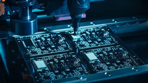
Innovations In Small Batch PCB Design And Fabrication
The landscape of printed circuit board (PCB) design and fabrication has undergone significant transformations in recent years, particularly in the realm of small batch production. This shift is driven by the increasing demand for rapid prototyping, customization, and the need for cost-effective solutions in various industries. Innovations in small batch PCB design and fabrication have played a pivotal role in meeting these demands, offering numerous advantages over traditional large-scale manufacturing processes.
One of the most notable advancements in small batch PCB production is the advent of advanced computer-aided design (CAD) software.
These tools have revolutionized the way engineers and designers approach PCB layout, enabling them to create intricate and highly optimized designs with greater ease and precision. The integration of simulation and analysis features within these software packages allows for the early detection of potential issues, thereby reducing the likelihood of costly errors during the fabrication process. Consequently, this has led to a significant reduction in the time and resources required to bring a new product to market.
In addition to CAD software, the development of automated manufacturing techniques has further streamlined the small batch PCB fabrication process.
Automated pick-and-place machines, for instance, have drastically improved the accuracy and speed of component placement on PCBs. These machines are capable of handling a wide variety of components, from surface-mount devices (SMDs) to through-hole components, ensuring that even the most complex designs can be assembled with minimal human intervention. This level of automation not only enhances production efficiency but also minimizes the risk of human error, resulting in higher quality and more reliable PCBs.
Moreover, the adoption of additive manufacturing technologies, such as 3D printing, has opened up new possibilities for small batch PCB production.
3D printing allows for the creation of complex geometries and customized designs that would be difficult or impossible to achieve using traditional subtractive manufacturing methods. This technology is particularly beneficial for prototyping and low-volume production runs, as it enables rapid iteration and testing of new designs without the need for expensive tooling or setup costs. As a result, companies can quickly and affordably develop and refine their products, ultimately accelerating the innovation cycle.
Another significant innovation in small batch PCB fabrication is the use of advanced materials and substrates.
Traditional PCBs are typically made from fiberglass-reinforced epoxy laminate, but recent advancements have introduced a range of alternative materials, such as flexible polymers and high-frequency laminates. These materials offer unique properties that can enhance the performance and durability of PCBs, making them suitable for a wider range of applications. For example, flexible PCBs can be bent and folded to fit into compact or irregularly shaped enclosures, while high-frequency laminates are ideal for high-speed communication devices.
Furthermore, the rise of online PCB manufacturing services has democratized access to small batch production capabilities.
These platforms allow designers and engineers to upload their PCB designs, receive instant quotes, and place orders for small quantities of PCBs with just a few clicks. This convenience has made it easier for startups, hobbyists, and small businesses to bring their ideas to life without the need for significant upfront investment. Additionally, many of these services offer value-added features, such as design for manufacturability (DFM) checks and technical support, ensuring that even those with limited experience can achieve professional-quality results.
In conclusion, the innovations in small batch PCB design and fabrication have significantly enhanced the efficiency, flexibility, and accessibility of the production process. Through the integration of advanced CAD software, automated manufacturing techniques, additive manufacturing technologies, and the use of novel materials, the industry has been able to meet the growing demand for rapid prototyping and customized solutions. As these technologies continue to evolve, they will undoubtedly pave the way for even greater advancements in the field of PCB design and fabrication.