Smart PCB Assembly Techniques for High-Yield Electronics Production
Key Takeaways
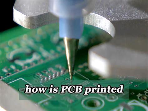
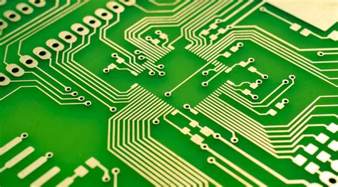
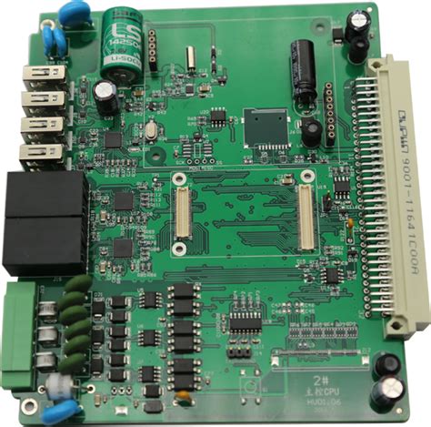
Modern PCB assembly processes rely on automation and precision engineering to achieve high yields in electronics manufacturing. Central to this is automated pick-and-place systems, which ensure micron-level accuracy in component positioning, reducing human error and accelerating throughput. For PCBA (Printed Circuit Board Assembly), precision soldering—including reflow and wave techniques—maintains electrical integrity while minimizing thermal stress on sensitive components.
Tip: Regularly calibrate soldering equipment to adapt to varying component sizes and thermal profiles, ensuring consistent joint quality across batches.
A critical focus area is thermal management, where improper heat distribution can lead to latent defects. Implementing embedded thermal sensors and heat-resistant materials mitigates risks, particularly in high-power applications. To further optimize yields, manufacturers deploy statistical process control (SPC) paired with automated optical inspection (AOI) systems.
| Factor | Traditional Approach | Smart Assembly |
|---|---|---|
| Component Placement | Manual alignment | Robotic vision systems |
| Defect Detection | Post-production testing | Real-time AOI monitoring |
| Soldering Consistency | Operator-dependent | Closed-loop temperature control |
Data-driven quality control strategies, such as cross-functional failure mode analysis, identify root causes of defects early, aligning with zero-defect manufacturing goals. By integrating advanced testing protocols—like in-circuit testing (ICT) and functional validation—PCBA lines achieve >99.5% reliability in high-volume production. This holistic approach ensures scalability without compromising the long-term durability of assembled circuits.
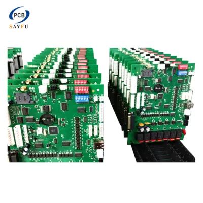
Automated PCB Assembly for High Yields
Modern PCB assembly processes leverage automated systems to achieve high-yield production in electronics manufacturing. By integrating PCBA (Printed Circuit Board Assembly) lines with robotic pick-and-place machines, manufacturers ensure micron-level accuracy in component placement, reducing human error and accelerating throughput. Advanced vision-guided systems align surface-mount devices (SMDs) with precision, while real-time feedback loops adjust parameters to maintain consistency across batches.
The adoption of closed-loop control mechanisms in PCB assembly enables dynamic optimization of solder paste application and reflow profiles, critical for minimizing voids or cold joints. Automated optical inspection (AOI) systems further enhance quality by scanning boards for defects like misalignments or solder bridges before downstream processes. This proactive defect detection slashes rework rates, ensuring PCBA outputs meet stringent reliability standards.
To sustain high yields, manufacturers combine data-driven analytics with modular PCB assembly workflows. Machine learning algorithms predict equipment wear, schedule preventive maintenance, and fine-tune placement sequences for complex layouts. Such integration not only boosts output but also scales efficiently for high-volume orders, solidifying automated PCBA as the backbone of modern electronics production.
Precision Soldering Techniques for Reliable PCBs
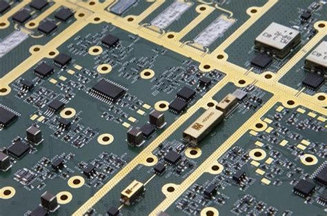
Achieving consistent solder joints is critical in PCB assembly processes, particularly for high-volume PCBA manufacturing. Modern techniques like reflow soldering and selective soldering leverage precise temperature controls to minimize thermal stress on sensitive components. For example, nitrogen-assisted reflow ovens reduce oxidation, ensuring cleaner connections for fine-pitch ICs and BGAs. Advanced systems integrate real-time thermal profiling to monitor solder paste behavior, preventing defects like cold joints or tombstoning.
Automated solder paste dispensers, paired with vision-guided placement systems, ensure micron-level accuracy in depositing solder alloys. This precision is vital for applications requiring high-density interconnects, such as industrial control boards. Post-soldering, automated optical inspection (AOI) and X-ray systems validate joint integrity, flagging micro-cracks or voids that compromise long-term reliability.
To balance speed and quality, manufacturers often adopt hybrid approaches—combining wave soldering for through-hole components with laser soldering for heat-sensitive parts. Such strategies align with PCB assembly best practices, ensuring robust electrical performance while meeting stringent industry standards like IPC-A-610. By refining these techniques, PCBA workflows achieve repeatable results, directly contributing to higher yields in electronics production.
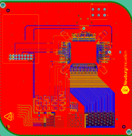
Optimize PCB Component Placement Accuracy
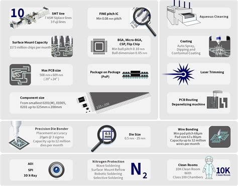
Achieving micron-level precision in PCB assembly begins with optimizing component placement accuracy, a critical factor influencing both yield rates and long-term circuit reliability. Modern PCBA lines leverage automated optical inspection (AOI) systems paired with high-speed pick-and-place machines to ensure components align within ±25µm tolerances, even for 01005 packages or fine-pitch BGAs. Advanced machine learning algorithms dynamically adjust placement parameters based on real-time feedback, compensating for thermal expansion or substrate warping during high-volume runs.
To minimize misalignment risks, engineers prioritize solder paste stencil design—ensuring optimal aperture ratios—and validate component libraries with 3D modeling tools to prevent footprint mismatches. Additionally, integrating vision-guided robotics with multi-spectral imaging reduces errors caused by polarity reversals or skewed orientations. For mixed-technology boards combining SMT and through-hole components, staggered placement sequences prevent mechanical interference while maintaining throughput. By refining these variables, manufacturers reduce rework costs by up to 40% and enhance first-pass yield metrics in PCB assembly workflows.
Thermal Management Solutions in PCB Production
Effective thermal management is critical in modern PCB assembly processes, particularly for high-density and power-intensive designs. As PCBA components shrink and power demands rise, managing heat dissipation ensures long-term reliability and prevents performance degradation. Key strategies include using thermal vias to transfer heat between layers, integrating copper pours for improved conductivity, and selecting substrates with low thermal resistance, such as metal-core or ceramic-based boards.
Advanced PCB assembly lines now employ infrared reflow ovens with precise temperature profiling, minimizing thermal stress on sensitive components like BGAs or QFNs. For high-power applications, engineers often incorporate heat sinks or active cooling systems, paired with thermally conductive adhesives like those found in Hobart thermal solutions. Additionally, finite element analysis (FEA) software enables predictive modeling of heat distribution, allowing optimization before prototyping.
By balancing material selection, layout design, and process controls, manufacturers achieve uniform thermal profiles across PCBA units, reducing warping and solder joint failures. This integration of thermal management into PCB assembly workflows not only enhances product durability but also aligns with stringent quality benchmarks for aerospace, automotive, and industrial electronics.
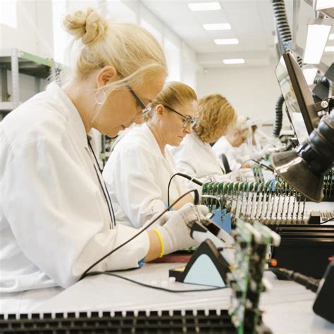
Quality Control Strategies for Mass PCB Assembly
Effective PCB assembly workflows in high-volume environments demand multilayered quality assurance protocols to balance speed and reliability. At the core of modern PCBA processes, automated optical inspection (AOI) systems scan boards at critical stages, flagging misalignments, solder bridging, or missing components with micron-level precision. Complementing these tools, X-ray inspection verifies hidden connections in ball grid arrays (BGAs) and under shields, ensuring integrity in complex layouts.
For consistency, statistical process control (SPC) tracks production metrics—such as solder paste volume and reflow oven profiles—to identify deviations before defects escalate. Advanced PCB assembly lines integrate machine learning algorithms that analyze historical defect data, refining placement accuracy and solder joint quality iteratively.
Equally critical is traceability, achieved through barcode or RFID tagging, which links each board to its component lot numbers and test results. This enables rapid root-cause analysis during failure investigations. Finally, in-circuit testing (ICT) and functional testing simulate real-world operating conditions, stress-testing power delivery, signal integrity, and thermal performance to meet reliability benchmarks. By harmonizing these strategies, manufacturers minimize rework cycles while maintaining <2% defect rates in PCBA outputs.
Minimizing Defects in Automated PCB Processes
Achieving near-zero defect rates in PCB assembly requires a systematic approach that combines process optimization with real-time monitoring. Modern PCBA lines leverage machine vision systems to detect misaligned components or solder paste irregularities at micron-level precision, catching errors before reflow soldering. Implementing statistical process control (SPC) tools helps identify deviations in placement speed, nozzle pressure, or feeder alignment, enabling corrective adjustments during high-volume runs.
Advanced PCB assembly workflows integrate automated optical inspection (AOI) and X-ray testing at multiple checkpoints, particularly for fine-pitch components like BGAs or QFNs. These systems cross-reference data against CAD models to flag discrepancies in solder joint integrity or tombstoning. For thermally sensitive assemblies, dynamic thermal profiling ensures reflow ovens maintain optimal temperature gradients, minimizing voids or cold joints.
To further reduce defects, manufacturers are adopting machine learning algorithms that analyze historical production data to predict and prevent failure patterns. For example, correlating humidity levels with solder bridging incidents allows preemptive environmental controls. Collaboration between design and manufacturing teams—supported by tools like design-for-manufacturability (DFM) guidelines—ensures component footprints and pad geometries align with PCBA equipment capabilities, reducing placement inaccuracies.
By combining these strategies, automated PCB assembly lines achieve defect rates below 50 ppm while maintaining throughput speeds exceeding 30,000 components per hour.
Smart PCB Assembly Boosts Manufacturing Yields
Modern PCB assembly processes leverage intelligent automation to achieve unprecedented production efficiency. By integrating real-time monitoring systems with PCBA lines, manufacturers can dynamically adjust parameters such as solder paste application and component alignment, reducing errors that traditionally lead to rework. For instance, automated optical inspection (AOI) systems paired with machine learning algorithms detect micron-level misalignments during PCB assembly, ensuring consistent placement accuracy across high-volume batches.
Another critical factor is the synchronization of thermal profiling with soldering stages. Advanced ovens maintain precise temperature gradients during PCBA reflow, minimizing thermal stress on sensitive components like BGAs or QFNs. This not only enhances joint reliability but also cuts defects by up to 30% in complex multilayer boards. Furthermore, closed-loop feedback mechanisms in smart PCB assembly lines enable rapid correction of deviations, such as excess solder paste deposition, before they escalate into costly failures.
By merging these technologies, manufacturers achieve yield rates exceeding 99% in optimized environments. The result is a seamless production workflow where speed and precision coexist, directly translating to lower per-unit costs and faster time-to-market for electronics OEMs.
Advanced Testing Methods for Circuit Reliability
Ensuring PCB assembly reliability demands rigorous testing protocols that validate both functionality and longevity. In-circuit testing (ICT) remains a cornerstone, using precision probes to measure electrical parameters and detect shorts, opens, or component mismatches in PCBA units. For complex boards, automated optical inspection (AOI) systems scan solder joints and component alignment at micron-level resolutions, flagging defects like tombstoning or insufficient solder paste. Thermal stress tests, such as thermal cycling, simulate extreme operating conditions to identify weak points in materials or connections—a critical step for electronics deployed in harsh environments.
Emerging technologies like 3D X-ray inspection enable non-destructive analysis of hidden connections, such as ball grid arrays (BGAs), ensuring integrity in high-density designs. Additionally, functional testing replicates real-world workloads to verify signal integrity and power distribution under load. These methods align with industry benchmarks like IPC-A-610, which outlines acceptance criteria for solder quality and component placement. By integrating these advanced techniques, manufacturers reduce field failure rates while maintaining compliance with aerospace, automotive, and medical-grade standards—key for PCB assembly workflows prioritizing zero-defect outcomes.
Conclusion
The evolution of PCB assembly processes underscores the critical role of integrating automation with precision engineering to achieve high-yield electronics manufacturing. By leveraging PCBA advancements—such as automated component placement systems and AI-driven inspection protocols—manufacturers can significantly reduce human error while scaling production. Modern techniques like laser soldering and reflow profiling ensure consistent joint integrity, directly enhancing circuit reliability in high-volume environments.
Effective thermal management strategies, including optimized heat dissipation designs and advanced materials, further mitigate risks of component failure during operation. Pairing these with rigorous in-circuit testing and AOI (Automated Optical Inspection) creates a闭环 quality control system, essential for minimizing defects in PCB assembly workflows. For deeper insights into multilayer board fabrication, refer to this comprehensive guide.
Ultimately, the synergy between smart PCBA technologies and data-driven process refinements enables manufacturers to balance speed, accuracy, and cost-efficiency. As industry demands grow, adopting these methodologies will remain pivotal for sustaining competitive advantage in electronics production.
FAQs
How does automated PCB assembly improve production yields?
Automated pick-and-place systems achieve micron-level accuracy in component placement, reducing human error. Integrated vision systems verify orientation and soldering quality in real-time, ensuring consistent PCBA outputs across high-volume batches.
What soldering techniques ensure reliability in PCB assembly?
Reflow soldering with precise thermal profiling maintains joint integrity, while selective soldering targets heat-sensitive components. Advanced nitrogen atmospheres during soldering minimize oxidation, enhancing PCBA longevity in harsh environments.
Why is thermal management critical during PCB assembly?
Effective heat dissipation prevents component degradation and warping. Automated thermal imaging identifies hotspots early, allowing design adjustments like thermal vias or heatsink integration to optimize PCBA performance under load.
How do manufacturers minimize defects in automated PCB assembly lines?
Statistical process control (SPC) monitors variables like solder paste volume and placement pressure. Combining AOI (Automated Optical Inspection) with X-ray testing catches hidden flaws, ensuring <1% defect rates in mature PCBA workflows.
What testing methods validate PCB assembly reliability for mission-critical applications?
In-circuit testing (ICT) verifies electrical parameters, while boundary scan checks component communication. Environmental stress testing simulates operating conditions, confirming PCBA durability through temperature cycling and vibration tests.
Optimize Your Production Line Today
For tailored PCB assembly solutions integrating these advanced techniques, please click here to consult our engineering team.