Smart Workflow Strategies for High-Yield PCBA Manufacturing

Key Takeaways
Effective PCBA production relies on balancing automation, precision, and data-driven oversight to achieve optimal results. Modern PCB assembly workflows integrate smart quality control systems that utilize machine vision and real-time analytics to identify defects at micron-level tolerances. By adopting modular automation in solder paste application and component placement, manufacturers reduce human error while accelerating throughput.
A critical consideration is the synchronization of PCBA stages—from design validation to final testing—ensuring seamless transitions between phases. For instance, embedding predictive maintenance protocols in pick-and-place machinery minimizes downtime, while AI-powered inspection tools correlate process parameters with defect patterns.
| Traditional Approach | Smart Workflow Strategy |
|---|---|
| Manual solder inspection | Automated optical inspection (AOI) |
| Fixed process parameters | Adaptive machine learning algorithms |
| Reactive defect management | Real-time defect root-cause analysis |
Transitioning from isolated processes to interconnected systems enables holistic yield optimization. Key metrics such as first-pass yield (FPY) and mean time between failures (MTBF) improve significantly when PCB assembly lines leverage IoT-enabled devices for continuous feedback. This strategic alignment not only reduces operational costs but also ensures scalability for high-mix, low-volume production demands. The following sections delve deeper into specific techniques for automating PCBA processes and integrating intelligent quality assurance frameworks.

Automating PCBA Assembly Processes
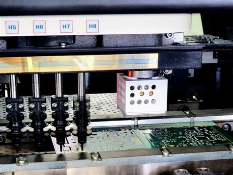
Modern PCB assembly lines achieve peak efficiency through strategic automation, combining robotic precision with intelligent process design. By integrating pick-and-place systems and AI-driven solder paste inspection (SPI), manufacturers minimize human error while accelerating throughput. Automated optical inspection (AOI) systems further enhance PCBA quality by detecting microscopic defects in real time, such as misaligned components or insufficient solder joints.
Tip: For high-mix production environments, modular automation tools allow rapid reconfiguration between PCB assembly batches, reducing downtime by up to 40% compared to fixed systems.
Advanced conveyor systems synchronized with machine learning algorithms optimize workflow pacing, balancing speed with precision. Closed-loop feedback mechanisms adjust parameters like reflow oven temperatures or component placement pressure, ensuring consistent output across varying PCBA designs. This approach not only reduces cycle times but also cuts material waste by 12–18%, according to industry benchmarks.
Transitioning to automated PCBA workflows requires upfront investment but delivers long-term ROI through predictive maintenance and data transparency. For instance, IoT-enabled machines generate actionable insights on tool wear or calibration drift, enabling preemptive adjustments before defects occur. By aligning automation with lean manufacturing principles, factories achieve scalable, defect-resistant PCB assembly processes tailored for high-yield production.
Precision PCB Assembly Techniques
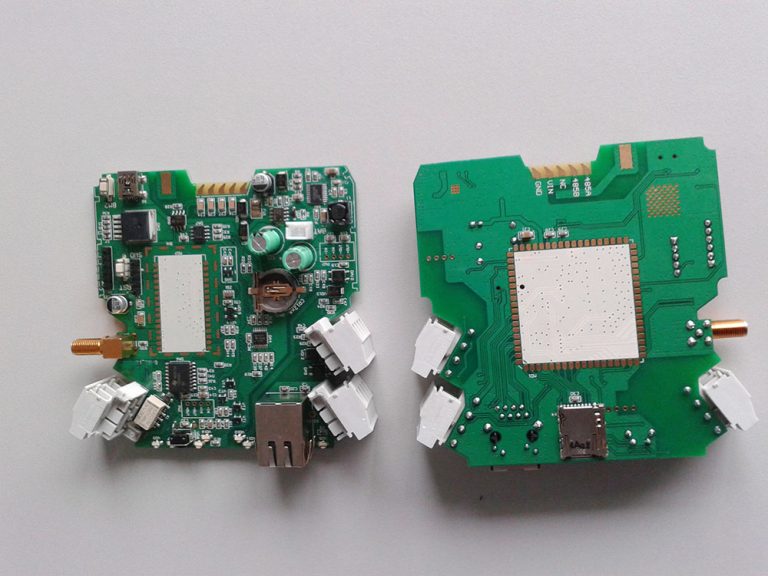
Achieving consistent quality in PCB assembly requires meticulous attention to component placement accuracy and solder joint integrity. Modern PCBA lines employ automated pick-and-place systems calibrated to micron-level precision, ensuring components align perfectly with pad geometries. Advanced surface-mount technology (SMT) processes leverage reflow ovens with dynamic thermal profiling to eliminate cold joints while preventing thermal stress on sensitive ICs. For high-density interconnects (HDIs), laser-drilled microvias and sequential lamination techniques maintain signal integrity in complex multilayer boards.
To mitigate defects, manufacturers integrate real-time solder paste inspection (SPI) systems that verify deposit volume and alignment before component placement. This proactive approach reduces rework by 30–40% in typical PCBA workflows. Additionally, nitrogen-assisted soldering minimizes oxidation during reflow, enhancing joint reliability for fine-pitch components like BGAs and QFNs.
Material selection also plays a critical role: low-loss dielectrics and high-tg substrates ensure stability under thermal cycling, while halogen-free solder masks align with environmental regulations. By harmonizing these techniques with data-driven process controls, PCB assembly lines achieve defect rates below 50 ppm, directly supporting yield optimization goals outlined in broader production strategies.
Smart Quality Control Systems Integration
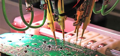
Integrating smart quality control systems into PCBA production lines has become a critical driver for achieving near-zero defect rates while maintaining operational efficiency. Modern systems combine automated optical inspection (AOI) with machine learning algorithms to analyze solder joint integrity, component placement accuracy, and trace alignment in real time. By embedding sensors directly within PCB assembly equipment, manufacturers gain granular visibility into process variations, enabling immediate corrections before defects propagate downstream.
Advanced platforms now utilize predictive analytics to cross-reference inspection data with historical performance metrics, identifying patterns that correlate with yield losses. For instance, high-precision X-ray inspection systems can detect hidden flaws like voids in ball grid arrays (BGAs) or microcracks in multilayer boards, ensuring compliance with aerospace and medical-grade reliability standards. This integration extends beyond defect detection, feeding critical insights back into PCBA workflows to refine pick-and-place calibration, reflow oven profiles, and testing protocols.
The synergy between intelligent quality control and precision PCB assembly techniques reduces manual verification by up to 70%, accelerating cycle times without compromising accuracy. Real-time dashboards provide operators with actionable metrics, from first-pass yield rates to component-level failure trends, fostering continuous improvement across production batches.
Maximizing Yield Through Process Optimization
Effective PCBA manufacturing relies on refining production workflows to achieve optimal yield rates. Central to this effort is the integration of data-driven process controls that monitor critical parameters in PCB assembly, from solder paste application to component placement accuracy. By implementing real-time feedback loops, manufacturers can instantly adjust variables like reflow oven temperatures or pick-and-place machine alignment, reducing deviations before they escalate into defects.
A key strategy involves optimizing SMT (Surface Mount Technology) processes through predictive maintenance and machine learning algorithms. These tools analyze historical production data to forecast potential bottlenecks in PCBA lines, enabling preemptive adjustments. For instance, panelization techniques can minimize material waste while ensuring consistent solder joint quality across multiple boards.
Additionally, standardized workflows for PCB assembly reduce variability between batches. Techniques like design-for-manufacturability (DFM) reviews and thermal profiling ensure components withstand assembly stresses. By synchronizing these steps with smart quality control systems, manufacturers achieve a balance between speed and precision, directly improving yield metrics.
Finally, continuous process validation through statistical process control (SPC) identifies subtle trends in PCBA production, allowing teams to address root causes of defects systematically. This approach not only elevates yield but also strengthens long-term process reliability, ensuring cost efficiencies without compromising on output quality.

Defect Reduction Strategies in Electronics Manufacturing
Effective defect management in PCBA manufacturing requires a multi-layered approach combining process refinement and predictive analytics. By integrating PCB assembly protocols with real-time monitoring systems, manufacturers can identify deviations at critical stages, such as solder paste application or component placement. Advanced inspection tools like automated optical inspection (AOI) and X-ray imaging enable precise detection of micro-defects, ensuring early intervention before errors propagate downstream.
Optimizing material handling and storage conditions further minimizes risks like moisture absorption or component misalignment, which account for 15-20% of PCBA defects. Implementing statistical process control (SPC) methodologies helps stabilize production variables, while machine learning algorithms analyze historical defect patterns to predict failure hotspots. For instance, adjusting reflow oven profiles based on thermal data reduces tombstoning and solder bridging by up to 35%.
Transitioning to standardized workflows across PCB assembly lines ensures consistency, particularly when scaling production. Cross-functional teams should collaborate to audit process flows, addressing bottlenecks that compromise yield rates. By aligning defect prevention with PCBA quality benchmarks, manufacturers achieve measurable improvements in reliability while maintaining cost-efficiency—a critical balance in high-volume electronics manufacturing.

Cost-Effective Automation for PCBA Production
Implementing cost-effective automation in PCBA production requires balancing technological investment with tangible returns. Modern PCB assembly lines increasingly integrate modular automation systems—such as programmable pick-and-place machines and AI-driven solder paste dispensers—to streamline workflows without overextending budgets. These systems reduce manual labor costs by up to 40% while maintaining high-precision assembly standards critical for complex multilayer boards.
A key strategy involves deploying scalable robotic solutions that adapt to varying production volumes. For instance, collaborative robots (cobots) excel in repetitive tasks like component insertion, minimizing human error and accelerating throughput. Pairing these with real-time monitoring software ensures immediate detection of anomalies, reducing material waste. Companies like CE3 Electronics leverage such integrations to optimize PCBA workflows, achieving defect rates below 0.1% even in high-mix environments.
Transitioning to automated optical inspection (AOI) systems further enhances cost efficiency. These tools perform microscopic defect analysis at speeds unattainable by manual checks, ensuring compliance with ISO 9001 standards. By aligning automation with data-driven process optimization, manufacturers achieve shorter lead times and higher yields, solidifying automation as a strategic investment rather than an operational expense.
Workflow Intelligence in Circuit Board Assembly
Modern PCB assembly workflows increasingly rely on intelligent systems to synchronize design, component placement, and testing phases. By integrating PCBA-specific automation tools with real-time data analytics, manufacturers achieve tighter control over production variables such as solder paste deposition accuracy and thermal profiling. For instance, machine vision systems paired with adaptive algorithms can detect micron-level deviations in surface-mount technology (SMT) processes, triggering immediate corrections to prevent downstream defects.
Transitioning from static workflows to dynamic, data-driven models enables factories to optimize line balancing. Advanced manufacturing execution systems (MES) analyze cycle times and equipment utilization, automatically rerouting tasks during bottlenecks. This agility is critical in high-mix environments where flexible PCB assembly lines must accommodate rapid product changeovers without sacrificing yield.
Central to workflow intelligence is the unification of automated optical inspection (AOI) and in-circuit testing (ICT) data. By correlating defect patterns with process parameters, teams identify root causes 30% faster, reducing rework cycles. Additionally, predictive maintenance algorithms monitor pick-and-place machinery health, cutting unplanned downtime by up to 22%. Such integrations ensure PCBA production remains responsive to both quality benchmarks and shifting demand curves.
Data-Driven Quality Assurance Methods
Modern PCBA manufacturing increasingly relies on statistical process control (SPC) and machine learning algorithms to identify defect patterns before they escalate. By integrating PCB assembly data streams—from solder paste inspection (SPI) to automated optical inspection (AOI)—manufacturers create predictive models that flag anomalies in real time. For instance, thermal profiling data from reflow ovens can correlate with solder joint quality, enabling adjustments to heating zones that reduce voiding risks by up to 40%.
Advanced systems leverage PCBA test results and failure mode databases to prioritize corrective actions. A leading EMS provider reported a 28% yield improvement after implementing AI-driven root cause analysis, which cross-referenced historical defect maps with current production variables. This approach minimizes human bias while accelerating first-pass yield optimization.
To maintain consistency, real-time dashboards track critical metrics like component placement accuracy and solder volume deviations, feeding insights back into PCB assembly workflows. Such closed-loop systems not only reduce rework costs but also refine tolerance thresholds for future batches, ensuring quality assurance evolves alongside design complexity.

Conclusion
In modern PCB assembly ecosystems, implementing intelligent workflow strategies proves critical for achieving sustainable production excellence. By integrating automated placement systems with adaptive process controls, manufacturers can maintain micron-level accuracy across high-volume PCBA lines while compensating for material variances. The convergence of machine vision inspection and predictive analytics creates self-optimizing feedback loops that preemptively address potential defect vectors – from solder paste deposition anomalies to component misalignment. Organizations adopting these methodologies often realize 30-50% reductions in post-reflow rework cycles, directly translating to improved throughput yields. Crucially, workflow intelligence extends beyond the production floor, requiring synchronization between design-phase simulations and real-world manufacturing parameters. This holistic approach ensures that PCBA operations not only meet current quality benchmarks but also possess the agility to adapt to evolving component miniaturization trends and regulatory requirements without costly retooling delays.
FAQs
How does automation improve efficiency in PCB assembly?
Automation streamlines PCBA processes by integrating robotic placement systems and AI-driven inspection tools, reducing manual intervention. This minimizes human error while accelerating throughput, particularly in high-volume production environments.
What role does precision play in PCBA manufacturing?
Precision in PCB assembly ensures components are placed with micron-level accuracy, critical for complex designs like high-density interconnect (HDI) boards. Advanced pick-and-place machines and laser-aligned soldering systems maintain consistency, directly impacting yield rates.
Can intelligent quality control reduce defects?
Yes. Smart systems combine automated optical inspection (AOI) and real-time analytics to detect anomalies early. By flagging issues like solder bridging or misalignment during PCBA stages, manufacturers achieve defect rates below 0.1% in optimized workflows.
How do data-driven methods lower operational costs?
Analyzing production metrics—such as cycle times and component waste—identifies bottlenecks. For example, predictive maintenance on PCB assembly equipment cuts downtime by up to 30%, aligning with cost-effective automation strategies.
What safeguards ensure workflow intelligence scalability?
Modular automation frameworks allow seamless integration of new technologies, such as IoT-enabled monitoring or machine learning algorithms. This adaptability future-proofs PCBA lines against evolving industry standards.
Ready to Optimize Your PCBA Workflow?
For tailored solutions in PCB assembly that prioritize yield and cost efficiency, please click here to explore advanced manufacturing services tailored to your project’s needs.