SMT patch basics analysis
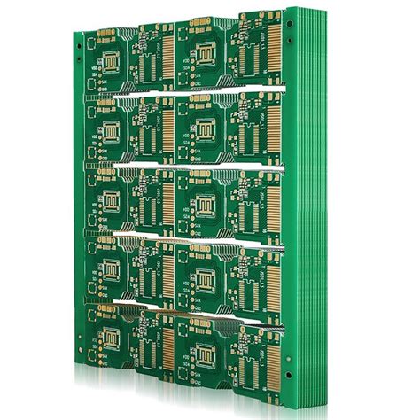
SMT patch refers to the abbreviation of a series of process flows based on PCB. PCB (Printed Circuit Board) is a printed circuit board.
SMT is the abbreviation of surface mount technology (surface mount technology), which is the most popular technology and process in the electronic assembly industry. Electronic circuit surface mount technology (Surface Mount Technology, SMT) is called surface mount or surface mounting technology. It is a circuit assembly technology that mounts pinless or short-lead surface mount components (abbreviated as SMC/SMD, Chinese called sheet components) on the surface of a printed circuit board (Printed Circuit Board, PCB) or other substrates, and assembles them by soldering or dip soldering.
In general, the electronic products we use are designed by PCB plus various capacitors, resistors and other electronic components according to the designed circuit diagram, so various electrical appliances require various SMT patch processing technologies to process.
Basic SMT process
Solder paste printing–> Parts mounting–> Reflow soldering–> AOI optical inspection–> Repair–> Board separation
Electronic products pursue miniaturization, and the perforated plug-in components used before can no longer be reduced. Electronic products have more complete functions, and the integrated circuits (ICs) used no longer have perforated components, especially large-scale, highly integrated ICs, which have to use surface mount components. With mass production and automated production, manufacturers must produce high-quality products at low cost and high output to meet customer needs and enhance market competitiveness. The development of electronic components, the development of integrated circuits (ICs), and the diversified application of semiconductor materials. The electronic technology revolution is imperative and pursues international trends. It can be imagined that when the production process of international CPU and image processing device manufacturers such as Intel and AMD has been refined to 20 nanometers, the development of SMT surface assembly technology and processes is also a situation that cannot be avoided.
Advantages of SMT patch processing: high assembly density, small size and light weight of electronic products, the size and weight of patch components are only about 1/10 of traditional plug-in components. Generally, after using SMT, the size of electronic products is reduced by 40%~60%, and the weight is reduced by 60%~80%. High reliability and strong vibration resistance. Low solder joint defect rate. Good high-frequency characteristics. Reduced electromagnetic and radio frequency interference. Easy to automate and improve production efficiency. Reduce costs by 30%~50%. Save materials, energy, equipment, manpower, time, etc.
It is precisely because of the complexity of the process flow of SMT patch processing that many SMT patch processing factories have emerged, specializing in SMT patch processing. In Shenzhen, thanks to the vigorous development of the electronics industry, SMT patch processing has achieved the prosperity of an industry.

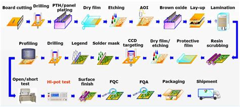
Process
The basic process components of SMT include: silk screen printing (or dispensing), mounting (curing), reflow soldering, cleaning, testing, and rework
- Silk screen printing: Its function is to print solder paste or patch glue on the pad of the PCB to prepare for the welding of components. The equipment used is a silk screen printer (screen printer), which is located at the forefront of the SMT production line.
- Dispensing: It is to drip glue on the fixed position of the PCB board. Its main function is to fix the components to the PCB board. The equipment used is a dispensing machine, which is located at the forefront of the SMT production line or behind the detection equipment.
- Mounting: Its function is to accurately install the surface mounted components to the fixed position of the PCB. The equipment used is a patch machine, which is located behind the screen printer in the SMT production line.
- Curing: Its function is to melt the patch glue so that the surface mounted components and the PCB board are firmly bonded together. The equipment used is a curing furnace, which is located behind the patch machine in the SMT production line.
- Reflow soldering: Its function is to melt the solder paste so that the surface mounted components and the PCB board are firmly bonded together. The equipment used is a reflow soldering furnace, which is located behind the patch machine in the SMT production line.
- Cleaning: Its function is to remove the soldering residues such as flux that are harmful to the human body on the assembled PCB board. The equipment used is a cleaning machine, which can be in an unfixed position, online or offline.
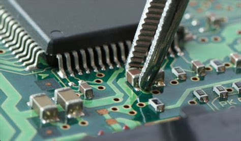
- Inspection: Its function is to inspect the welding quality and assembly quality of the assembled PCB board. The equipment used includes magnifying glass, microscope, in-circuit tester (ICT), flying probe tester, automatic optical inspection (AOI), X-RAY inspection system, functional tester, etc. The position can be configured at a suitable place on the production line according to the needs of the inspection.
- Rework: Its function is to rework the PCB board that has failed in the inspection. The tools used are soldering iron, rework workstation, etc. It can be configured at any position in the production line.
SMT process
Single-sided assembly
Incoming material inspection => Silk screen solder paste (smearing SMT glue) => SMT => Drying (curing) => Reflow soldering => Cleaning => Inspection => Rework
Double-sided assembly
A: Incoming material inspection => Silk screen solder paste (smearing SMT glue) on the A side of PCB => SMT Silk screen solder paste (smearing SMT glue) on the B side of PCB => SMT => Drying => Reflow soldering (preferably only on the B side => Cleaning => Inspection => Rework).
B: Incoming material inspection => Screen printing solder paste on PCB A side (applying SMD glue) => SMD => Drying (curing) => Reflow soldering on A side => Cleaning => Flip board = Apply SMD glue on PCB B side => SMD => Curing => Wave soldering on B side => Cleaning => Inspection => Rework)
This process is suitable for reflow soldering on PCB A side and wave soldering on B side. This process is suitable for SMDs assembled on PCB B side when there are only SOT or SOIC (28) pins or less.
Single-sided mixed assembly process
Incoming material inspection => PCB A-side screen printing solder paste (apply SMD glue) => SMD => drying (curing) => reflow soldering => cleaning => plug-in => wave soldering => cleaning => inspection => rework
Double-sided mixed assembly process
A: Incoming material inspection => PCB B-side SMD glue => SMD => curing => flip board => PCB A-side plug-in => wave soldering => cleaning => inspection => rework
First paste and then plug-in, suitable for the situation where there are more SMD components than discrete components
B: Incoming material inspection => PCB A-side plug-in (pin bending) => flip board => PCB B-side SMD glue => SMD => curing => flip board => wave soldering => cleaning => inspection => rework
First plug-in and then paste, suitable for the situation where there are more discrete components than SMD components
C: Incoming material inspection => PCB A-side screen printing solder paste => SMD => drying => reflow soldering => plug-in, pin bending => Turn over => Apply SMD glue to PCB B side => SMD => Curing => Turn over => Wave soldering => Cleaning => Inspection => Rework A side mixed assembly, B side mounting.
D: Incoming material inspection => Apply SMD glue to PCB B side => SMD => Curing => Turn over => Silk screen solder paste on PCB A side => SMD => Reflow soldering on A side => Plug-in => Wave soldering on B side => Cleaning => Inspection => Rework A side mixed assembly, B side mounting. First paste SMD on both sides, reflow soldering, then insert, wave soldering E: Incoming material inspection => Silk screen solder paste (smear patch glue) on the B side of PCB => Smear => Drying (curing) => Reflow soldering => Flip board => Silk screen solder paste on the A side of PCB => Smear => Drying = Reflow soldering 1 (local soldering can be used) => Plug-in => Wave soldering 2 (if there are few insert components, manual soldering can be used) => Cleaning => Inspection => Rework A side mounting, B side mixed mounting.
Double-sided assembly process
A: Incoming material inspection, silk screen solder paste (smear patch glue) on the A side of PCB, Smear, drying (curing), reflow soldering on the A side, cleaning, flip board; silk screen solder paste (smear patch glue) on the B side of PCB, Smear, drying, reflow soldering (preferably only on the B side, cleaning, inspection, rework)
This process is suitable for mounting large SMDs such as PLCC on both sides of the PCB.
B: Incoming material inspection, screen printing solder paste on the A side of the PCB (applying SMD glue), SMD, drying (curing), reflow soldering on the A side, cleaning, flipping; applying SMD glue on the B side of the PCB, SMD, curing, wave soldering on the B side, cleaning, inspection, rework) This process is suitable for reflow on the A side of the PCB.
Thin film printed circuits
This type of thin film circuit is generally printed on PET with silver paste. There are two processes for pasting electronic components on this type of thin film circuit. One is the traditional process, namely the 3-glue method (red glue, silver glue, encapsulation glue) or the 2-glue method (silver glue, encapsulation glue), and the other is the new process, namely the 1-glue method—as the name suggests, it is to use one glue to complete the pasting of electronic components, instead of using 3 glues or 2 glues. The key to this new process is to use a new type of conductive glue, which has the conductive properties and process properties of solder paste; when used, it is fully compatible with the current SMT solder paste brushing operation method, without adding any equipment.
Reduce Failures
Manufacturing, handling, and printed circuit assembly (PCA) testing can subject packages to many mechanical stresses that can cause failures. As grid array packages get larger, it becomes increasingly difficult to set safety levels for these steps.
For many years, packages have been characterized using a monotonic bending point test method described in IPC/JEDEC-9702, Monotonic Flexural Characterization of Horizontal Interconnects on a Board. This test method describes the fracture strength of horizontal interconnects on a printed circuit board under bending loads. However, this test method does not determine the maximum allowable strain.
One of the challenges of manufacturing and assembly, especially for lead-free PCAs, is the inability to directly measure stress on solder joints. The most widely used metric to describe the risk of an interconnect component is the strain on the printed circuit board adjacent to the component, as described in IPC/JEDEC-9704, Guide for Strain Testing of Printed Wiring Boards.
Several years ago, Intel recognized this problem and began developing a different test strategy to replicate the worst-case bending conditions that occur in the field. Other companies such as Hewlett-Packard also realized the benefits of other test methods and began to consider similar ideas as Intel. The method has gained interest as more chip manufacturers and customers realize the value of determining the strain limit to minimize mechanically induced failures during manufacturing, handling and testing.
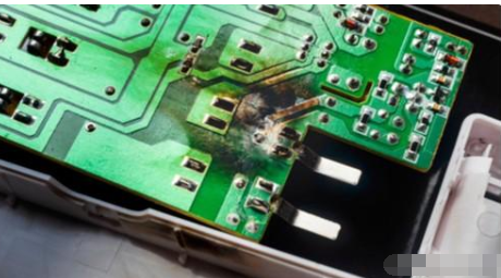
As the use of lead-free devices has expanded, user interest has also increased; many users face quality issues.
As interest has increased, IPC has felt the need to help other companies develop test methods that can ensure that BGAs are not damaged during manufacturing and testing. This work has been completed by the IPC 6-10d SMT Attachment Reliability Test Methods Working Group and the JEDEC JC-14.1 Packaged Device Reliability Test Methods Subcommittee.
The test method specifies eight contact points arranged in a circular array. The PCA with a BGA mounted in the center of the printed circuit board is mounted with the component facing down on the support pins and the load applied to the back of the BGA. The strain gages are placed adjacent to the component according to the recommended gage layout of IPC/JEDEC-9704.
The PCA is bent to the relevant tension levels, and the degree of damage caused by bending to these tension levels can be determined through failure analysis. The tension level without damage can be determined through iterative methods. This is the tension limit.
Packaging materials
Usually the packaging materials are plastics and ceramics. The heat sink part of the component may be composed of metal. The pins of the component are divided into leaded and lead-free.