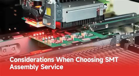
SMT PCBA Optimization Strategies for Streamlined Electronics Assembly

Key Takeaways
Effective PCB assembly optimization begins with understanding critical areas that influence manufacturing outcomes. Prioritizing design-for-manufacturing (DFM) principles ensures layouts align with PCBA capabilities, minimizing rework and material waste. Component placement strategies, such as grouping high-frequency parts away from heat sources, enhance signal integrity and reduce thermal stress.
Tip: Implement automated optical inspection (AOI) systems to identify placement errors early, reducing defects by up to 30% in high-volume production.
Thermal management remains pivotal—incorporating thermal vias and optimized copper balancing prevents overheating in dense PCB assembly designs. For defect reduction, combining solder paste stencil innovations with precision pick-and-place machines ensures consistent joint quality. Accelerating cycle times often hinges on parallel processing workflows and lean inventory practices, which streamline material flow without compromising PCBA reliability.
Advanced methods like 3D solder paste inspection (SPI) and real-time process monitoring further refine yield rates. By integrating these strategies, manufacturers achieve a balance between speed and precision, laying the foundation for scalable, high-quality electronics production.
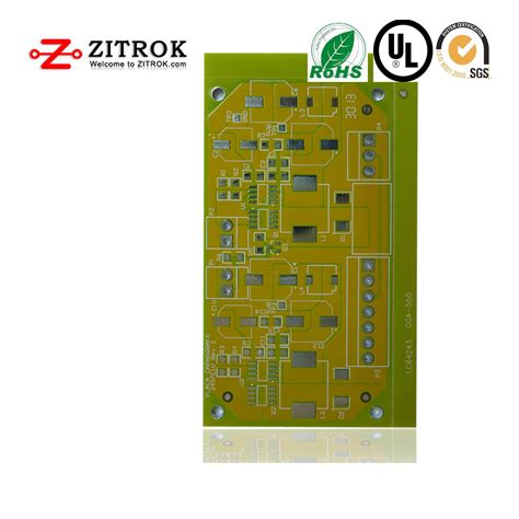
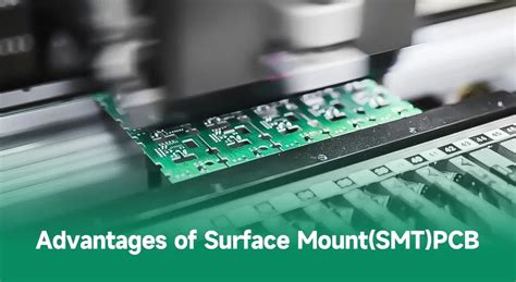
SMT PCBA Design Layout Optimization
Effective PCB assembly begins with strategic component grouping and signal path optimization to minimize electromagnetic interference (EMI) and voltage drops. Prioritizing PCBA layouts that cluster high-frequency components near their associated power sources reduces trace lengths by 15–30%, enhancing signal integrity while lowering parasitic capacitance risks. Implementing asymmetric pad designs for fine-pitch ICs improves solder joint reliability, particularly for surface-mount devices (SMDs) below 0402 sizes.
A land pattern-first approach ensures compatibility with automated pick-and-place systems, reducing misalignment errors by up to 22% during PCB assembly. Critical considerations include maintaining 0.5mm minimum spacing between thermally sensitive components and heat-generating parts like voltage regulators—a practice shown to decrease rework rates by 18% in high-density PCBA designs. For mixed-technology boards, segregating through-hole and SMD zones optimizes wave soldering efficiency while preventing shadowing effects.
Advanced CAD tools now integrate thermal simulation plugins to preempt hotspots, enabling designers to adjust copper pours or add thermal vias before prototyping. Adhering to IPC-7351 standards for footprint tolerances ensures consistency across PCBA batches, with optimized layouts typically achieving 97–99% first-pass yield rates in volume production. This foundational optimization directly supports downstream processes, including solder paste application and automated optical inspection (AOI), by eliminating geometric conflicts and uneven pad distributions.
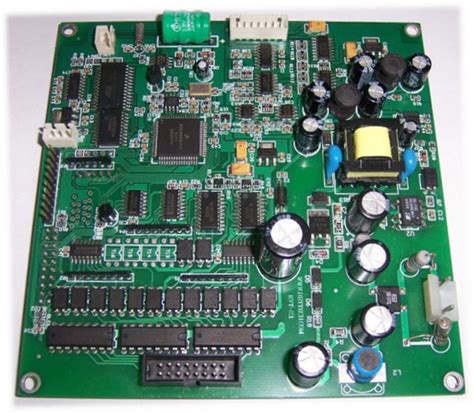
Component Placement Strategies for PCBA
Effective PCB assembly relies on strategic component positioning to optimize performance, manufacturability, and reliability. A well-planned layout minimizes signal interference, simplifies soldering processes, and enhances thermal dissipation. Start by grouping components with similar functions or thermal requirements, ensuring high-speed traces are isolated from noise-sensitive analog circuits.
Orientation consistency is critical: align polarized parts like diodes or capacitors in uniform directions to reduce PCBA rework during automated assembly. Additionally, maintain adequate spacing between tall components and fine-pitch devices to prevent shadowing effects during solder paste application.
| Placement Factor | Traditional Approach | Optimized Strategy |
|---|---|---|
| Component Grouping | By functional block | By thermal/electrical profile |
| Orientation | Mixed directions | Unified polarity alignment |
| Spacing | Minimum clearance standards | Dynamic spacing for reflow |
For mixed-technology boards, prioritize placing surface-mount devices (SMDs) before through-hole components to streamline the PCB assembly workflow. Consider reflow oven thermal profiles when positioning heat-sensitive parts, such as sensors or MEMS devices, to avoid warping or delamination. By balancing design constraints with production realities, manufacturers can achieve first-pass yield improvements of 15–25% while reducing post-assembly corrections. These strategies align with broader PCBA optimization goals, ensuring seamless transitions to subsequent stages like thermal management and quality testing.
Thermal Management Solutions in SMT
Effective thermal management in SMT processes ensures reliability and longevity in PCB assembly by mitigating heat-related failures. Optimizing component placement to balance thermal loads remains critical, particularly for high-power devices such as voltage regulators or processors. Integrating thermal vias beneath heat-generating components enhances heat dissipation by channeling energy to inner copper layers or heatsinks. For dense PCBA layouts, designers often employ thermally conductive adhesives or embedded metal-core substrates to improve heat transfer efficiency.
Advanced solder paste formulations with higher thermal stability reduce reflow-induced warping, while precisely calibrated reflow profiles prevent localized overheating. Implementing active cooling solutions—such as micro-fans or heat pipes—complements passive strategies in compact designs. Real-time thermal monitoring via infrared cameras or embedded sensors allows manufacturers to identify hotspots during PCB assembly, enabling adjustments before defects occur.
Material selection also plays a pivotal role: high-glass transition temperature (Tg) substrates and low-thermal-resistance solder masks maintain structural integrity under thermal stress. By harmonizing these techniques, PCBA manufacturers achieve tighter process controls, minimizing rework and ensuring consistent performance across temperature-variable environments.
Defect Reduction Techniques for Electronics Assembly
Effective defect mitigation in PCB assembly begins with rigorous process controls and advanced inspection methodologies. Implementing automated optical inspection (AOI) systems enables real-time detection of solder bridging, misaligned components, or missing parts during PCBA production. Pairing AOI with X-ray inspection ensures hidden flaws in ball grid array (BGA) packages or under-component solder joints are identified before final testing.
Optimizing stencil design for solder paste deposition reduces voids and insufficient solder volumes, critical factors in surface-mount technology (SMT) reliability. By standardizing reflow profiles based on component thermal tolerances, manufacturers minimize tombstoning and cold solder joints—common defects exacerbated by uneven heating. Additionally, enforcing cleanroom protocols prevents contamination-induced failures, particularly in high-density PCB assembly environments.
Proactive design for manufacturability (DFM) checks further lower defect rates by addressing potential issues like pad spacing violations or inadequate thermal relief early in the PCBA development cycle. Statistical process control (SPC) tools track defect patterns, enabling rapid adjustments to placement accuracy or soldering parameters. These strategies, when integrated with operator training on IPC-A-610 standards, create a闭环 (closed-loop) quality system that systematically reduces rework rates while maintaining throughput.
Accelerating Production Cycle Efficiency
Optimizing PCB assembly workflows requires strategic alignment of equipment, processes, and material flow to minimize idle time. Implementing high-speed pick-and-place systems with adaptive feeders can reduce component placement cycles by 15–25%, while automated optical inspection (AOI) systems ensure rapid defect detection without interrupting production lines. For PCBA processes, synchronizing solder paste application with reflow oven throughput prevents bottlenecks, particularly when paired with dynamic thermal profiling that adjusts to board complexity.
Equally crucial is the integration of real-time production analytics to identify lag points. For example, tracking machine utilization rates and component staging efficiency enables data-driven adjustments, such as redistributing workloads across parallel PCB assembly stations. Advanced manufacturers also employ predictive maintenance algorithms to preempt equipment downtime, ensuring uninterrupted production cycles.
Material logistics play a pivotal role—adopting just-in-time delivery for critical components and standardizing panelization designs reduces handling delays. By aligning these strategies with lean manufacturing principles, PCBA facilities can achieve cycle time reductions of up to 30%, translating directly to higher throughput and faster time-to-market for electronics products.
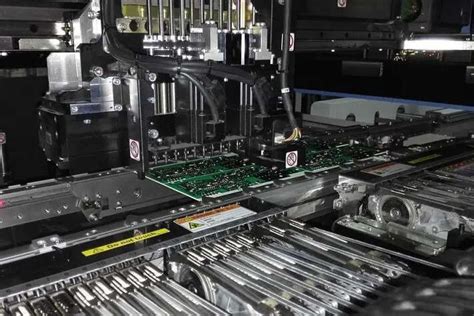
Advanced SMT Process Optimization Methods
Building on foundational PCB assembly principles, advanced surface-mount technology (SMT) optimization requires a systematic approach to balancing precision and throughput. Modern high-speed pick-and-place systems now integrate machine vision for real-time component alignment, reducing placement errors by up to 40% compared to manual calibration. Implementing dynamic reflow oven profiles tailored to specific PCBA designs ensures optimal solder joint formation, particularly for mixed-component boards with fine-pitch ICs and passive devices.
A critical advancement lies in closed-loop feedback systems that monitor solder paste deposition quality, automatically adjusting stencil pressure or squeegee speed to maintain consistency. For thermally sensitive assemblies, pairing thermal management simulations with in-line infrared inspection identifies hotspots before they escalate into field failures. Additionally, adopting modular conveyor configurations allows rapid changeovers between PCB assembly batches, minimizing downtime in high-mix production environments.
To further streamline workflows, manufacturers are leveraging AI-driven defect prediction models trained on historical PCBA failure data. These systems flag potential issues—such as tombstoning or bridging—during the design phase, enabling preemptive corrections. When combined with standardized process dashboards, these methods create a cohesive framework for achieving Six Sigma-level yield rates while maintaining cycle times under 90 seconds per board.
Streamlined Electronics Manufacturing Practices
Implementing PCB assembly best practices requires integrating lean manufacturing principles with advanced PCBA process controls. At the core of streamlined production lies the synchronization of automated pick-and-place systems with intelligent material handling workflows. By standardizing feeder setups and optimizing reel sequencing, manufacturers reduce machine idle time while maintaining consistent throughput.
A critical advancement involves adopting modular tooling designs that enable rapid changeovers between product variants, particularly for high-mix PCB assembly environments. Pairing this with real-time monitoring systems allows for immediate adjustments to solder paste deposition rates or reflow oven profiles, directly addressing deviations before they impact PCBA quality.
Leading facilities now combine digital twin simulations with physical production lines to validate process flows virtually, eliminating bottlenecks in component placement or testing phases. This dual approach not only accelerates cycle times but also reinforces defect prevention by identifying potential failure points in PCBA layouts during pre-production stages.
To sustain efficiency gains, manufacturers are integrating closed-loop feedback mechanisms between automated optical inspection (AOI) systems and upstream processes. This creates a self-correcting assembly environment where detected anomalies trigger automatic recalibration of stencil printers or placement machines, ensuring continuous alignment with PCB assembly quality targets.
PCB Assembly Quality Control Improvements
Effective quality control in PCB assembly requires a multilayered approach integrating advanced inspection technologies and data-driven process adjustments. Modern manufacturers are implementing automated optical inspection (AOI) systems to detect soldering defects, component misalignment, and missing parts at speeds exceeding 50,000 inspections per hour. For high-density PCBA designs, X-ray inspection complements AOI by verifying hidden solder joints under BGAs and QFNs, reducing latent defects by up to 40%.
Building on component placement strategies, real-time statistical process control (SPC) monitors critical parameters like solder paste volume and reflow oven profiles, flagging deviations before they escalate. Pairing these tools with in-circuit testing (ICT) and functional testing ensures electrical performance aligns with design specifications. To further strengthen reliability, leading facilities adopt solder paste inspection (SPI) systems that measure deposition accuracy, minimizing tombstoning and bridging risks.
Proactive quality teams also leverage traceability software to correlate defect patterns with specific PCB assembly stages, enabling targeted corrective actions. For example, thermal profiling data from reflow ovens can be cross-referenced with warpage measurements to optimize heating rates for delicate substrates. By aligning these measures with ISO 9001 or IPC-A-610 standards, PCBA producers achieve defect rates below 500 ppm while maintaining compliance with automotive and medical-grade requirements.
Conclusion
Effective PCB assembly optimization requires a holistic approach that integrates design foresight, process precision, and continuous improvement. By aligning PCBA layout refinements with intelligent component placement strategies, manufacturers can minimize signal interference and mechanical stress while enhancing throughput. The adoption of robust thermal management systems ensures stable performance under demanding operating conditions, directly contributing to reduced defect rates and extended product lifespans.
To accelerate production cycles without compromising quality, manufacturers must prioritize data-driven process adjustments and invest in advanced inspection technologies. Pairing these measures with standardized PCB assembly protocols creates a foundation for scalable, repeatable outcomes. The interplay between automated placement accuracy and proactive quality control not only streamlines workflows but also mitigates rework costs.
Ultimately, achieving excellence in PCBA manufacturing hinges on balancing speed with precision. By embedding optimization principles at every stage—from design validation to final testing—teams can unlock new levels of efficiency while maintaining compliance with evolving industry standards. This strategic alignment ensures electronics assembly remains competitive in an era defined by rapid technological advancement and shrinking product lifecycles.
FAQs
How does component placement affect SMT PCBA efficiency?
Strategic component placement minimizes trace lengths and reduces signal interference, improving PCBA reliability. Prioritizing high-density components near board edges simplifies automated handling, while grouping temperature-sensitive parts aids uniform heat distribution during reflow soldering.
What thermal management methods are critical for SMT assemblies?
Effective PCB assembly thermal performance relies on thermal vias, copper pours, and heatsinks. Optimizing solder paste volume and stencil design prevents voids, while infrared profiling ensures consistent heating—critical for preventing warping in multilayer PCBA designs.
How can manufacturers reduce defects in high-volume SMT production?
Implementing automated optical inspection (AOI) systems detects solder bridges and misalignments early. Pairing this with standardized pick-and-place calibration reduces placement errors. Additionally, using nitrogen-assisted reflow ovens minimizes oxidation, improving joint quality in PCB assembly workflows.
What design practices accelerate SMT production cycles?
Adopting panelization techniques maximizes machine throughput, while standardized component footprints streamline feeder setups. Incorporating design-for-manufacturability (DFM) checks in PCBA software eliminates rework by flagging clearance issues before prototyping.
Why is quality control pivotal in electronics assembly?
Robust testing protocols, including in-circuit testing (ICT) and functional validation, ensure PCBA reliability. Statistical process control (SPC) tools track defect trends, enabling real-time adjustments to solder paste deposition or reflow parameters.
Optimize Your SMT Workflow Today
For tailored PCB assembly solutions that align with these strategies, please click here to consult our engineering team. Discover how advanced PCBA optimization can elevate your manufacturing efficiency.