Solidworks flexible pcb
Designing Flexible PCBs in SolidWorks: A Step-by-Step Guide
Designing flexible PCBs in SolidWorks requires a meticulous approach, combining both the mechanical and electrical aspects of design to ensure functionality and manufacturability.
The process begins with understanding the unique characteristics of flexible PCBs, which differ significantly from their rigid counterparts. Flexible PCBs are designed to bend and twist, making them ideal for applications where space constraints and dynamic movements are prevalent. This inherent flexibility necessitates a different design strategy, one that SolidWorks is well-equipped to handle.
To start, it is essential to set up the SolidWorks environment correctly.
This involves configuring the software to accommodate the specific requirements of flexible PCB design. Begin by creating a new project and selecting the appropriate template that supports flexible materials. SolidWorks provides various tools and features tailored for PCB design, including the ability to define the board shape, layer stack-up, and material properties. These initial steps are crucial as they lay the foundation for the entire design process.
Once the environment is set up, the next step is to import or create the PCB layout.
This can be done by either importing an existing design from another CAD tool or by creating a new layout directly within SolidWorks. The software’s intuitive interface allows for precise placement of components, routing of traces, and definition of vias. It is important to consider the mechanical constraints and bending requirements during this phase. SolidWorks offers simulation tools that enable designers to visualize how the PCB will behave under various conditions, ensuring that the design meets the necessary flexibility criteria.
Transitioning from layout to 3D modeling, SolidWorks excels in providing a comprehensive view of the PCB in its final form.
The 3D model allows designers to check for potential interferences and ensure that the PCB fits within the intended enclosure. This step is particularly important for flexible PCBs, as their ability to bend and conform to different shapes can introduce unique challenges. By leveraging SolidWorks’ advanced modeling capabilities, designers can iterate on their designs, making adjustments as needed to achieve the desired fit and function.
As the design progresses, it is essential to perform thorough validation and testing.
SolidWorks offers a range of simulation tools that can be used to analyze the mechanical and thermal performance of the flexible PCB. These simulations help identify potential issues such as stress concentrations, excessive bending, and thermal hotspots. By addressing these issues early in the design process, designers can avoid costly revisions and ensure that the final product meets all performance requirements.
Finally, once the design is validated, the last step is to prepare the manufacturing files.
SolidWorks simplifies this process by providing tools to generate the necessary Gerber files, drill files, and assembly drawings. These files are critical for the fabrication and assembly of the flexible PCB. It is important to review these files carefully to ensure that all design specifications are accurately captured and that there are no errors that could impact the manufacturing process.
In conclusion, designing flexible PCBs in SolidWorks involves a series of well-defined steps, from setting up the environment and creating the layout to 3D modeling, validation, and preparation of manufacturing files. By following this step-by-step guide, designers can leverage SolidWorks’ powerful tools to create flexible PCBs that meet the demanding requirements of modern electronic applications. The integration of mechanical and electrical design within a single platform streamlines the process, ensuring a seamless transition from concept to production.
Best Practices for Creating Flexible PCB Layouts in SolidWorks
Creating flexible PCB layouts in SolidWorks requires a meticulous approach to ensure both functionality and manufacturability. To achieve optimal results, it is essential to adhere to best practices that streamline the design process and mitigate potential issues.
One of the first steps in this endeavor is to thoroughly understand the specific requirements and constraints of flexible PCBs.
Unlike rigid PCBs, flexible circuits must accommodate bending, folding, and dynamic movement, which necessitates careful consideration of material properties and mechanical stresses.
To begin with, selecting the appropriate materials is crucial.
Flexible PCBs typically use polyimide substrates due to their excellent thermal stability and flexibility. Ensuring that the chosen materials can withstand the intended operating environment is fundamental. Additionally, it is important to consider the thickness of the substrate and copper layers, as these factors directly influence the flexibility and durability of the PCB.
Once the material selection is finalized, the next step involves designing the layout with flexibility in mind.
One effective strategy is to incorporate curved traces instead of sharp angles. Sharp angles can act as stress concentrators, leading to potential failures when the PCB is bent. By using smooth, curved traces, the stress distribution is more even, enhancing the overall reliability of the circuit. Furthermore, maintaining consistent trace widths and spacing is essential to prevent issues such as impedance mismatches and signal integrity problems.
Another critical aspect is the placement of components.
In flexible PCB design, it is advisable to position components in areas that experience minimal bending. Placing components in the bend regions can lead to mechanical stress and potential damage. Instead, components should be located in flat or less flexible sections of the PCB. Additionally, using surface-mount technology (SMT) components can be beneficial, as they are generally more resilient to bending compared to through-hole components.
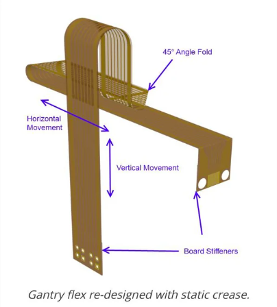
Transitioning to the routing phase, it is important to consider the bend radius of the flexible PCB.
The bend radius is the minimum radius that the PCB can be bent without causing damage. Adhering to the recommended bend radius for the chosen materials ensures that the PCB can flex without compromising its integrity. Moreover, incorporating teardrop pads at the junctions of traces and pads can help reduce stress concentrations and improve the mechanical robustness of the design.
Thermal management is another vital consideration in flexible PCB design.
Flexible circuits can be more susceptible to thermal expansion and contraction due to their thin and pliable nature. To address this, it is essential to design for adequate heat dissipation. This can be achieved by optimizing the placement of thermal vias and using appropriate copper weights. Additionally, conducting thermal simulations during the design phase can help identify potential hotspots and allow for proactive adjustments.
Finally, collaboration with the manufacturer is indispensable.
Engaging with the manufacturer early in the design process can provide valuable insights into the manufacturability of the flexible PCB. Manufacturers can offer guidance on material selection, layer stack-up, and other critical parameters. Moreover, they can help identify potential design issues that may not be apparent during the initial design phase.
In conclusion, creating flexible PCB layouts in SolidWorks demands a comprehensive understanding of material properties, mechanical stresses, and thermal management. By adhering to best practices such as selecting appropriate materials, designing with flexibility in mind, optimizing component placement, considering bend radius, and collaborating with manufacturers, designers can ensure the successful implementation of flexible PCBs. These practices not only enhance the reliability and performance of the final product but also streamline the design and manufacturing process, ultimately leading to more efficient and cost-effective solutions.

Integrating Flexible PCBs with Rigid Components in SolidWorks
Integrating flexible PCBs with rigid components in SolidWorks requires a nuanced understanding of both the software’s capabilities and the unique properties of flexible printed circuit boards.
Flexible PCBs, known for their ability to bend and conform to various shapes, offer significant advantages in modern electronic design, particularly in applications where space constraints and mechanical flexibility are paramount. SolidWorks, a leading CAD software, provides robust tools to model and simulate these complex assemblies, ensuring that designers can achieve both functionality and manufacturability.
To begin with, it is essential to recognize the distinct characteristics of flexible PCBs compared to their rigid counterparts.
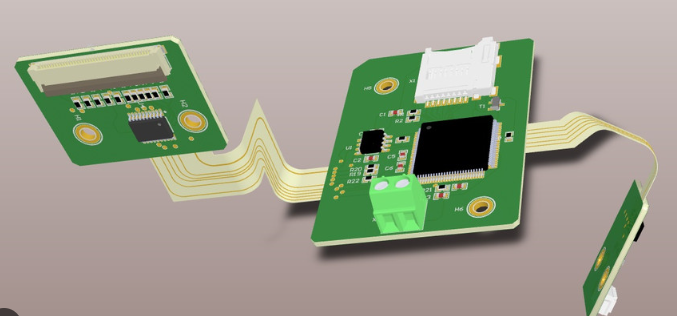
Flexible PCBs are typically made from materials like polyimide, which provide the necessary flexibility and durability. These materials allow the circuits to bend, fold, and twist without breaking, making them ideal for applications in wearable technology, medical devices, and compact consumer electronics. However, integrating these flexible elements with rigid components, such as connectors, sensors, and other electronic modules, presents unique challenges that must be addressed during the design phase.
SolidWorks offers a suite of tools that facilitate the integration of flexible and rigid components.
One of the key features is the ability to create multi-body parts, which allows designers to model both the flexible and rigid sections within a single part file. This approach ensures that the relationship between the different sections is accurately represented, enabling more precise simulations and analyses. Additionally, SolidWorks’ sheet metal tools can be adapted to model the bending and folding behavior of flexible PCBs, providing a visual and functional representation of how the PCB will behave in real-world applications.
Transitioning from the design to the simulation phase, SolidWorks Simulation provides powerful capabilities to analyze the mechanical behavior of flexible PCBs.
By applying appropriate material properties and boundary conditions, designers can simulate the bending, twisting, and stretching of the flexible PCB under various loads and constraints. This analysis is crucial for identifying potential failure points and ensuring that the design can withstand the mechanical stresses it will encounter during operation. Moreover, the ability to visualize the deformation of the flexible PCB in SolidWorks helps in optimizing the layout and placement of components, ensuring that they remain secure and functional even when the PCB is flexed.
Furthermore, SolidWorks’ integration with other tools, such as SolidWorks Electrical and CircuitWorks, enhances the design process by providing seamless collaboration between mechanical and electrical design teams. This integration ensures that the electrical schematics and PCB layouts are accurately reflected in the 3D model, reducing the risk of errors and improving overall design efficiency. Additionally, the ability to import and export data between SolidWorks and other PCB design software allows for a more streamlined workflow, facilitating the integration of flexible PCBs with rigid components.
In conclusion, the integration of flexible PCBs with rigid components in SolidWorks is a complex but manageable task, thanks to the software’s comprehensive set of tools and features. By leveraging SolidWorks’ capabilities for multi-body part modeling, mechanical simulation, and seamless collaboration between design teams, engineers can create innovative and reliable electronic products that meet the demands of modern applications. As technology continues to evolve, the ability to effectively integrate flexible and rigid components will remain a critical skill for designers, ensuring that they can deliver cutting-edge solutions that push the boundaries of what is possible.
Troubleshooting Common Issues in SolidWorks Flexible PCB Design
Designing flexible PCBs in SolidWorks can be a complex task, often fraught with various challenges that can impede progress. Understanding and troubleshooting these common issues is crucial for ensuring a smooth design process and achieving optimal results.
One of the primary issues encountered is the difficulty in accurately modeling the flexible regions of the PCB.
This often stems from the inherent complexity of simulating the bending and flexing behaviors of the material. To address this, it is essential to utilize the correct material properties and ensure that the bend radius is within the manufacturer’s specifications. Additionally, employing SolidWorks’ advanced simulation tools can provide a more accurate representation of the flexing behavior, thereby mitigating potential design flaws.
Another prevalent issue is the misalignment of components when transitioning from a rigid to a flexible section.
This misalignment can lead to connectivity problems and potential failures in the final product. To troubleshoot this, designers should meticulously check the alignment of components and ensure that the transition areas are properly defined. Using SolidWorks’ alignment tools can aid in maintaining the correct positioning of components, thereby reducing the risk of misalignment.
Thermal management is another critical aspect that often poses challenges in flexible PCB design.
The flexible nature of the PCB can lead to uneven heat distribution, which can adversely affect the performance and longevity of the components. To mitigate this, designers should conduct thorough thermal analysis using SolidWorks’ simulation capabilities. This allows for the identification of potential hotspots and the implementation of appropriate cooling solutions, such as heat sinks or thermal vias, to ensure even heat distribution.
Signal integrity is also a significant concern in flexible PCB design.
The bending and flexing of the PCB can introduce noise and signal degradation, which can compromise the functionality of the device. To address this, designers should pay close attention to the routing of high-speed signals and ensure that they are kept away from noisy components. Utilizing SolidWorks’ signal integrity analysis tools can help identify potential issues and allow for the optimization of signal paths to maintain signal integrity.
Furthermore, manufacturing constraints can often pose challenges in the design of flexible PCBs.
The unique properties of flexible materials require specific manufacturing processes, which can limit design options. To troubleshoot this, designers should collaborate closely with manufacturers to understand the limitations and capabilities of the manufacturing process. This collaboration can help in making informed design decisions that are both manufacturable and meet the desired performance criteria.
Lastly, documentation and communication issues can arise during the design process. Clear and comprehensive documentation is essential for ensuring that all stakeholders, including manufacturers and assembly teams, have a thorough understanding of the design. SolidWorks provides various tools for generating detailed documentation, including drawings and BOMs (Bill of Materials). Ensuring that these documents are accurate and up-to-date can prevent miscommunication and errors during the manufacturing and assembly stages.
In conclusion, while designing flexible PCBs in SolidWorks presents several challenges, understanding and addressing these common issues can significantly enhance the design process. By leveraging SolidWorks’ advanced tools and maintaining close collaboration with manufacturers, designers can overcome these challenges and achieve successful flexible PCB designs.


