Solve EMI problems through high-speed PCB control
With the decrease of signal rise time and the increase of signal frequency, the EMI problem of electronic products has been paid more and more attention by electronic engineers. The success of high-speed PCB design has made more and more attention to the contribution of EMI. Almost 60% of EMI problems can be controlled and solved by high-speed PCB.
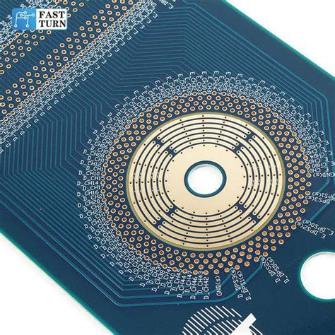
1 High-speed signal routing shielding rules
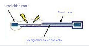
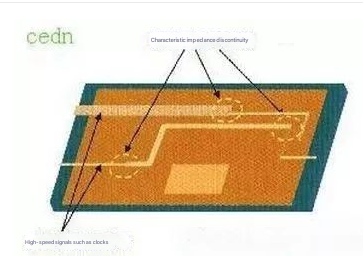
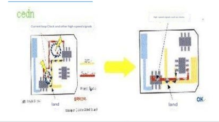
As shown in the figure above: In high-speed PCB design, key high-speed signal lines such as clocks need to be shielded. If they are not shielded or only partially shielded, EMI leakage will occur. It is recommended to punch holes for grounding every 1000mil for shielded lines. 2. Closed-loop routing rules for high-speed signals As the density of PCB boards increases, many PCB layout engineers are prone to this kind of mistakes during routing, as shown in the following figure:
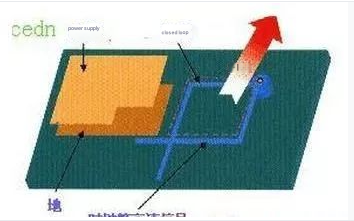
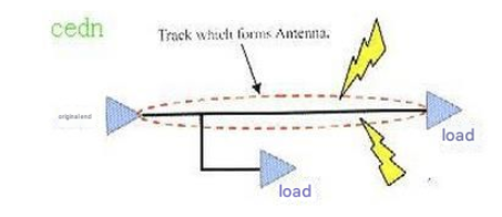
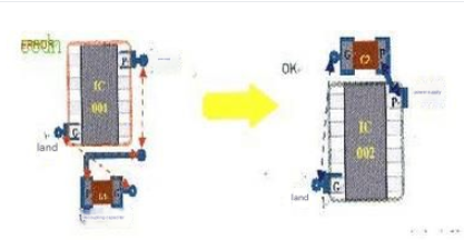
High-speed signal networks such as clock signals produce closed-loop results when routing on multi-layer PCBs. Such closed-loop results will produce loop antennas and increase the radiation intensity of EMI. 3. Open-loop routing rules for high-speed signals Rule 2 mentions that closed-loop high-speed signals will cause EMI radiation, and the same open-loop will also cause EMI radiation, as shown in the following figure:
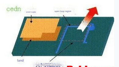
High-speed signal networks such as clock signals produce open-loop results when routing on multi-layer PCBs. Such open-loop results will produce linear antennas and increase the radiation intensity of EMI. We should also avoid this in design. 4 Continuous characteristic impedance rules for high-speed signals When switching between layers, high-speed signals must ensure the continuity of characteristic impedance, otherwise EMI radiation will increase, as shown in the following figure:
That is, the width of the wiring on the same layer must be continuous, and the impedance of the wiring on different layers must be continuous. 5 Routing direction rules for high-speed PCB design The wiring between two adjacent layers must follow the principle of vertical wiring, otherwise it will cause crosstalk between lines and increase EMI radiation, as shown in the following figure:
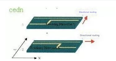
The adjacent wiring layers follow the horizontal and vertical wiring direction, and vertical wiring can suppress crosstalk between lines. 6 Topological structure rules in high-speed PCB design There are two most important contents in high-speed PCB design, namely the control of characteristic impedance of the circuit board and the design of topological structure under multi-load conditions. In the case of high speed, it can be said that the rationality of the topological structure directly determines the success or failure of the product.
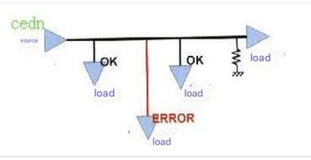
As shown in the figure above, this is the daisy chain topology we often use. This topology is generally suitable for several MHz. For high-speed topology, we recommend using a star-shaped symmetrical structure at the back end. 7 Resonance rules for routing length
Check whether the length of the signal line and the frequency of the signal constitute resonance, that is, when the wiring length is an integer multiple of 1/4 of the signal wavelength, this wiring will resonate, and the resonance will radiate electromagnetic waves and cause interference. 8 Return path rules
All high-speed signals must have a good return path. Try to minimize the return path of high-speed signals such as clocks. Otherwise, the radiation will be greatly increased, and the size of the radiation is proportional to the area surrounded by the signal path and the return path. 9 Rules for placing decoupling capacitors of devices
The placement of the decoupling capacitor is very important. An unreasonable placement will not achieve the decoupling effect at all. The principle of placing the decoupling capacitor is: close to the power pin, and the area surrounded by the power line and ground line of the capacitor is the smallest.