Solving Grounding Issues in PCB Design: A Comprehensive Guide
Introduction
Printed Circuit Board (PCB) design represents one of the most critical aspects of electronic product development, where proper grounding techniques often distinguish between a functional circuit and one plagued with noise, interference, and reliability issues. Grounding in PCBs serves as the reference point for all voltages in the system, provides return paths for currents, and plays a vital role in electromagnetic compatibility (EMC) performance. This 2000-word article explores the fundamental challenges of PCB grounding, analyzes common grounding problems, and provides practical solutions to achieve optimal grounding in modern electronic designs.
Understanding PCB Grounding Fundamentals
The Concept of Ground in Electronic Circuits
The term “ground” in electronic circuits refers to the reference point from which all other voltages are measured. Contrary to common misconception, ground doesn’t necessarily mean a connection to the earth—it serves as the common return path for electric current to complete its circuit. In PCB design, we typically deal with several ground types:
- Signal Ground: Reference for analog and digital signals
- Power Ground: Return path for power supply currents
- Chassis Ground: Physical connection to the metal enclosure
- Earth Ground: Actual connection to the earth (in some systems)
Ground Plane Importance
Modern PCBs typically incorporate ground planes—continuous layers of copper dedicated to grounding. These planes serve multiple functions:
- Low Impedance Return Path: Provides the shortest possible return current path, minimizing inductance
- Noise Reduction: Acts as a shield against electromagnetic interference (EMI)
- Heat Dissipation: Helps distribute and dissipate heat from components
- Signal Integrity Maintenance: Provides consistent reference for high-speed signals
Common PCB Grounding Problems
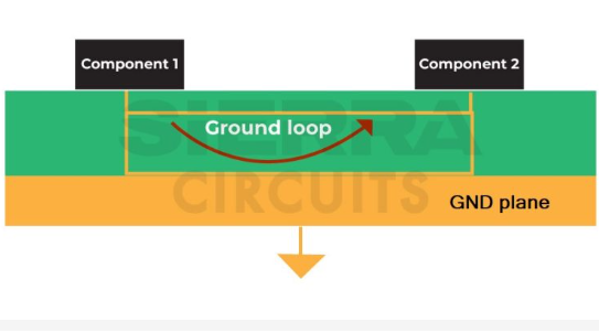
Ground Loops
Ground loops occur when multiple ground paths create circular conducting paths between different points supposedly at the same ground potential. These loops can:
- Act as antennas picking up electromagnetic interference
- Create voltage differences between supposedly grounded points
- Cause audible hum in audio systems or noise in measurement circuits
Impedance Issues
At high frequencies, even small inductances in ground paths can create significant impedance (XL = 2πfL). This impedance causes:
- Voltage drops along ground paths
- Inconsistent reference voltages across the board
- Radiated emissions as high-frequency currents seek alternative return paths
Mixed Signal Grounding Challenges
Combining analog and digital circuits on the same PCB presents unique grounding difficulties:
- Digital switching noise can couple into analog circuits
- High-speed digital return currents can modulate analog ground references
- Sensitive analog measurements require ultra-clean ground references
Split Plane Issues
While splitting ground planes for analog and digital sections seems logical, improper implementation can:
- Create return path discontinuities for high-frequency signals
- Increase radiation from the splits acting as slot antennas
- Cause impedance mismatches for high-speed signals crossing splits

Effective Grounding Solutions
Proper Ground Plane Design
- Use Continuous Ground Planes: For multilayer boards, dedicate entire layers to ground
- Minimize Plane Splits: Only split planes when absolutely necessary with proper bridging
- Multiple Vias: Use numerous ground vias to connect ground planes in multilayer boards
- Low Impedance Connections: Ensure solid connections between ground points
Mixed Signal Grounding Techniques
- Single-Point Grounding: Connect analog and digital grounds at a single point (usually at power supply)
- Partitioned Ground Planes: Physically separate analog and digital sections but maintain continuous ground plane
- Proper Component Placement: Group analog components together and digital components together
- Careful ADC/DAC Placement: Place bridging components (ADCs, DACs) at the ground connection point
High-Speed Design Considerations
- Return Path Analysis: Ensure every signal has a clear return path directly beneath it
- Avoid Ground Plane Splits Under High-Speed Signals: Maintain continuous reference plane
- Via Placement: Place ground vias adjacent to signal vias for layer transitions
- Decoupling Capacitors: Properly placed to provide high-frequency current return paths
Practical Implementation Guidelines
- Star Grounding: For low-frequency circuits, implement star grounding topology
- Separate Power and Signal Grounds: Join them at a single point near power supply
- Chassis Connection: Connect PCB ground to chassis at one point to avoid ground loops
- Testing and Verification: Use techniques like ground impedance measurement and thermal imaging
Advanced Grounding Techniques
Multi-board System Grounding
For systems with multiple PCBs:
- Single Ground Reference: Establish one board as the ground reference
- Daisy-chain Avoidance: Use star configuration for multiple board connections
- Isolation When Needed: Use opto-isolators or transformers when ground potential differences exist
RF Grounding Techniques
For radio frequency circuits:
- Short Ground Connections: Minimize inductance with extremely short paths
- Via Fences: Create walls of ground vias to contain RF energy
- Copper Pour: Extensive ground copper around RF components
- Shielding Cans: When necessary, with proper grounding
Verification and Testing
Ground Impedance Measurement
- Four-point Probe Method: For accurate low-impedance measurement
- Frequency Response Analysis: Measure impedance across frequency spectrum
- Time Domain Reflectometry: Identify discontinuities in ground paths
EMI/EMC Testing
- Radiated Emissions Testing: Verify ground effectiveness in containing EMI
- Conducted Emissions Testing: Evaluate power-ground noise coupling
- Susceptibility Testing: Ensure ground protects against external interference
Thermal Imaging
- Identify Current Crowding: Shows areas of excessive current density
- Hot Spot Detection: Reveals poor grounding or insufficient copper
Case Studies
Case 1: Digital Noise in Analog Circuit
A data acquisition system showed excessive noise in analog measurements. Analysis revealed:
- Problem: Digital return currents flowing through analog ground section
- Solution: Implemented partitioned ground plane with single connection point
- Result: 12dB improvement in signal-to-noise ratio
Case 2: Radiated Emissions Failure
A consumer product failed FCC radiated emissions testing:
- Problem: High-speed signals crossing ground plane splits
- Solution: Redesigned ground plane to maintain continuity under critical traces
- Result: Passed retest with 8dB margin
Case 3: Intermittent Communication Errors
A multi-board industrial controller showed random communication faults:
- Problem: Ground potential differences between boards creating timing errors
- Solution: Implemented single-point ground reference and optical isolation
- Result: Eliminated communication errors entirely
Future Trends in PCB Grounding
- Higher Frequency Challenges: As speeds increase, grounding becomes more critical
- 3D Printed Electronics: New manufacturing methods require adapted grounding approaches
- Flexible PCBs: Unique grounding considerations for bendable circuits
- AI-Assisted Design: Machine learning for optimal ground plane optimization
Conclusion
Proper PCB grounding remains both an art and a science, requiring careful consideration of electrical principles, practical constraints, and specific application requirements. By understanding fundamental grounding concepts, recognizing common problems, and implementing appropriate solutions, designers can create PCBs that deliver optimal performance, reliability, and EMC compliance. As electronic systems continue increasing in complexity and speed, mastery of grounding techniques will remain an essential skill for successful PCB design. The solutions presented in this article provide a solid foundation, but designers must always consider their specific context and be prepared to adapt these principles to unique challenges. Through careful implementation and thorough testing, grounding issues can be effectively solved, resulting in robust, high-performance electronic products.