Solving Multi-Channel Design Challenges in PCB Layout
Introduction
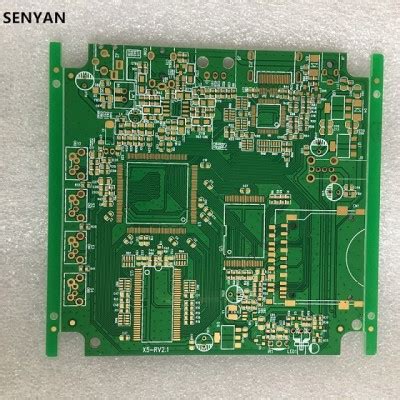
Printed Circuit Board (PCB) design has evolved significantly with the increasing complexity of electronic systems. One of the most challenging aspects of modern PCB design is managing multi-channel layouts, where multiple identical or similar signal paths must be routed efficiently while maintaining signal integrity, minimizing crosstalk, and ensuring manufacturability.
Multi-channel designs are common in applications such as:
- Data acquisition systems
- High-speed ADCs/DACs
- RF and communication systems
- Medical imaging devices
- Industrial automation
This article explores the key challenges in multi-channel PCB design and provides practical solutions to optimize performance, reduce errors, and improve efficiency.

Challenges in Multi-Channel PCB Design
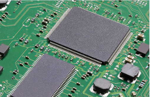
1. Signal Integrity and Crosstalk
In multi-channel designs, parallel signal paths can lead to crosstalk, where electromagnetic interference (EMI) from one channel affects another. This is especially problematic in high-speed and high-frequency designs.
Solution:
- Proper spacing and shielding – Maintain adequate distance between traces and use ground planes to isolate channels.
- Differential signaling – Use differential pairs to reduce noise susceptibility.
- Controlled impedance routing – Ensure impedance matching to prevent reflections.
2. Channel-to-Channel Skew
When signals travel through multiple channels, slight variations in trace lengths can cause timing skew, leading to synchronization issues in high-speed systems.
Solution:
- Length matching – Use serpentine routing to equalize trace lengths.
- Delay tuning – Adjust propagation delays using simulation tools.
- Group routing – Route related signals together to minimize skew.
3. Power Distribution and Noise
Multiple channels drawing power simultaneously can lead to ground bounce and power supply noise, degrading signal quality.
Solution:
- Decoupling capacitors – Place capacitors near ICs to stabilize power.
- Split power planes – Use separate power domains for sensitive circuits.
- Star grounding – Minimize ground loops by using a central grounding scheme.
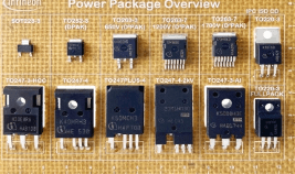
4. Thermal Management
High-density multi-channel PCBs generate significant heat, which can affect performance and reliability.
Solution:
- Thermal vias – Improve heat dissipation by adding vias under hot components.
- Copper pours – Use large copper areas to spread heat.
- Active cooling – Incorporate heatsinks or fans if necessary.
5. Manufacturing and Assembly Challenges
Complex multi-channel layouts increase the risk of manufacturing defects, such as solder bridges or misaligned components.
Solution:
- Design for Manufacturability (DFM) – Follow PCB manufacturer guidelines for trace width, spacing, and via sizes.
- Automated Optical Inspection (AOI) – Use AOI to detect assembly errors.
- Panelization – Optimize panel layouts for efficient fabrication.
Best Practices for Multi-Channel PCB Design
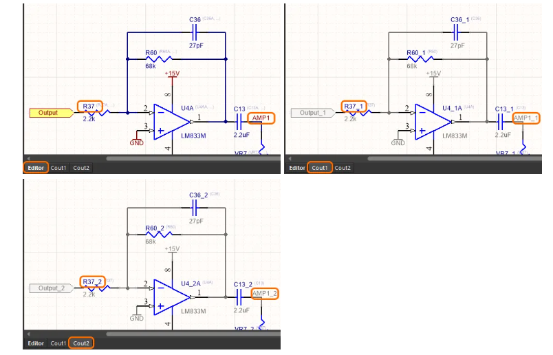
1. Modular Design Approach
- Break the PCB into functional blocks (e.g., one channel per section).
- Reuse validated sub-circuits to ensure consistency.
2. Use of Symmetry
- Mirror component placement and routing for identical channels.
- Simplifies design verification and reduces errors.
3. Simulation and Validation
- Perform signal integrity (SI) and power integrity (PI) simulations.
- Use 3D EM solvers to analyze crosstalk and radiation.
4. Automated Routing Tools
- Leverage auto-routing with constraints to ensure consistent channel routing.
- Use scripting (e.g., Python, SKILL) for repetitive tasks.
5. Documentation and Version Control
- Maintain clear design notes for each channel.
- Use Git or SVN to track changes in complex layouts.
Case Study: Multi-Channel ADC PCB Design
A common application of multi-channel design is in Analog-to-Digital Converter (ADC) systems, where multiple analog inputs must be digitized with minimal interference.
Problem: A 16-channel ADC system exhibited crosstalk and timing mismatches, leading to inaccurate readings.
Solution Implemented:
- Isolated Ground Planes – Separated analog and digital grounds.
- Matched Trace Lengths – Used length-tuning features in CAD tools.
- Shielded Routing – Added guard traces between sensitive signals.
Result:
- Crosstalk reduced by 20 dB.
- Timing skew minimized to <10 ps.
- Improved ADC accuracy by 15%.
Future Trends in Multi-Channel PCB Design
- AI-Assisted Layout Optimization – Machine learning can predict optimal routing paths.
- Advanced Materials – Low-loss dielectrics for high-frequency multi-channel designs.
- 3D Printed Electronics – Additive manufacturing for complex multi-layer PCBs.
Conclusion
Multi-channel PCB design presents unique challenges, but with careful planning, simulation, and adherence to best practices, engineers can achieve high-performance, reliable layouts. By leveraging modern CAD tools, simulation software, and modular design techniques, designers can overcome signal integrity, power distribution, and thermal issues while ensuring manufacturability.
As electronic systems continue to grow in complexity, mastering multi-channel PCB design will remain a critical skill for engineers working in high-speed, RF, and mixed-signal applications.