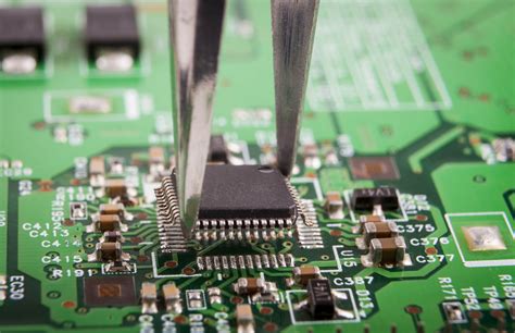
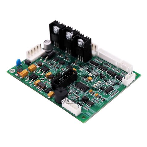
Special Process for PCB
As a person in the PCB industry, you must be proficient in PCB copying and PCB design related processes. Through the analysis and summary of our professional PCB copying experts, our professional PCB copying experts have come up with the following special processes for PCB processing, hoping to be helpful to people in the PCB industry.
- Additive Process
It refers to the process of directly growing local conductor lines with chemical copper layer on the surface of non-conductive substrate with the help of additional resist (see Circuit Board Information Magazine Issue 47 P.62 for details). The additive process used for PCB copying can be divided into full additive, semi-additive and partial additive methods. - Backpanels, Backplanes Support Board
It is a thicker circuit board (such as 0.093″, 0.125″), which is specially used for plugging and connecting other boards. The method is to first insert a multi-pin connector (Connector) into the tight through hole, but without soldering, and then connect the wires one by one on the guide pins of the connector passing through the board in a winding manner. A general PCB copy board can be inserted into the connector. Because this special board cannot be soldered through the through hole, but the hole wall and the guide pin are directly clamped and used, so its quality and aperture requirements are particularly strict, and the order volume is not large. General circuit board factories are unwilling and difficult to accept such orders. It has almost become a high-grade specialized industry in the United States.
- Build Up Process
This is a new field of thin multi-layer board method. The earliest enlightenment originated from IBM’s SLC process. The Yasu factory in Japan began trial production in 1989. The method is based on the traditional double-sided board. The two outer surfaces are first fully coated with liquid photosensitive precursors such as Probmer 52. After semi-hardening and photosensitive resolution, a shallow “photosensitive guide hole” (Photo-Via) connected to the next bottom layer is made. Then, chemical copper and electroplated copper are used to increase the conductor layer. After line imaging and etching, new wires and buried holes or blind holes interconnected with the bottom layer can be obtained. Repeatedly adding layers in this way will result in a multilayer board with the required number of layers. This method not only eliminates the expensive mechanical drilling costs, but also reduces the hole diameter to less than 10mil. In the past 5 to 6 years, various multilayer board technologies that break the tradition and adopt sequential layering have become famous under the continuous promotion of American, Japanese and European companies, and more than ten products have been launched on the market. In addition to the above-mentioned “photosensitive hole formation”, there are also different “hole formation” methods such as alkaline chemical biting holes for organic boards after removing the copper foil at the hole position, laser ablation, and plasma etching. In addition, a new type of “resin coated copper foil” coated with semi-hardened resin can also be used to make a thinner, denser, smaller and thinner multilayer board by sequential lamination. In the future, diversified personal electronic products will become the world of this truly thin and short multilayer board. - Cermet Ceramic powder is mixed with metal powder, and then an adhesive is added as a coating. It can be printed on the circuit board surface (or inner layer) in a thick or thin film manner as a “resistor” to replace the external resistor during assembly.
- Co-Firing
It is a process for the production of ceramic hybrid PCB circuit boards (Hybrid). The circuits printed with various precious metal thick film pastes (Thick Film Paste) on the small board are placed at high temperature for firing. The various organic carriers in the thick film paste are burned, leaving the circuits of precious metal conductors as interconnecting wires. - Crossover is the three-dimensional intersection of two wires on the crossover board, and the gap between the intersection points is filled with insulating medium. Generally, the green paint surface of a single-sided board with a carbon film jumper, or the wiring above and below the layer-building method are all such “crossovers”.
- Discreate Wiring Board PCB, Multi-Wiring Board
Another name for Multi-Wiring Board is that it is made by attaching round enameled wires to the board surface and adding through holes. The performance of this multi-wire board in high-frequency transmission lines is better than the flat square lines etched by ordinary PCB. - DYCOstrate plasma etching hole layering method
It is a build up process developed by Dyconex, a company located in Zurich, Switzerland. The copper foil at each hole position of the board surface is first etched away, and then placed in a closed vacuum environment, and filled with CF4, N2, and O2, so that it is ionized under high voltage to form a highly active plasma (Plasma), which is used to etch through the substrate at the hole position, and a patented method of tiny guide holes (less than 10mil) appears. Its commercial process is called DYCOstrate. - Electro-Deposited Photoresist
It is a new type of “photoresist” construction method, originally used for “electrodeposited paint” of metal objects with complex shapes, and has only recently been introduced to the application of “photoresist”. It uses electroplating to evenly plate the charged colloidal particles of photosensitive resin on the copper surface of the PCB circuit board as an anti-etching resist.
It has now begun to be mass-produced and used in the direct copper etching process of the inner layer board. This type of ED photoresist can be placed on the anode or cathode according to different operation methods, and is called “anodic electrodeposited photoresist” and “cathodic electrodeposited photoresist”.
It can also be divided into two types according to its different photosensitive principles: “photosensitive polymerization” (negative working) and “photosensitive decomposition” (positive working). At present, negative working ED photoresist has been commercialized, but it can only be used as a planar resist. It cannot be used for image transfer of outer layer boards due to the difficulty of photosensitizing through holes. As for the “positive ED” that can be used as the photoresist of the outer layer (because it is a photosensitive decomposition film, the hole wall is not sensitive enough but it has no effect), Japanese companies are still stepping up their efforts to launch commercial mass production, making it easier to make fine lines. This term is also called “electrophoretic photoresist”. - Flush Conductor Embedded Circuit, Flat Conductor
It is a special PCB copy board circuit board with a completely flat surface and all conductor circuits pressed into the board. The single-sided board is made by etching away the copper foil on the board surface by image transfer on the semi-cured substrate board. Then the board surface circuit is pressed into the semi-cured board by high temperature and high pressure, and the board resin can be hardened at the same time, making the circuit retracted into the surface and completely flat. Usually, on the surface of the retracted circuit of this board, a thin copper layer needs to be micro-etched to plate another 0.3mil nickel layer, a 20-micro-inch rhodium layer, or a 10-micro-inch gold layer, so that when performing sliding contact, the contact resistance can be lower and it is easier to slide. However, this method is not suitable for PTH to prevent the through hole from being squeezed during pressing, and it is not easy to achieve a completely smooth surface for this board. It cannot be used at high temperatures to prevent the circuit from being pushed out of the surface after the resin expands. This technology is also called Etch and Push method, and the finished board is called Flush-Bonded Board, which can be used for special purposes such as Rotary Switch and Wiping Contacts. - In addition to precious metal chemicals, glass powder needs to be added to the thick film paste (Poly Thick Film, PTF) printing paste to achieve condensation and adhesion effects during high-temperature incineration, so that the printing paste on the blank ceramic substrate can form a solid precious metal circuit system.
- Fully-Additive Process
It is a method of growing selective circuits on a completely insulated board surface by electroless metal deposition (mostly chemical copper), which is called “full additive process”. Another incorrect term is “Fully Electroless”.
- Hybrid Integrated Circuit
It is a circuit that prints precious metal conductive ink on a small ceramic thin substrate, and then burns the organic matter in the ink at high temperature, leaving the conductor circuit on the board surface, and can be soldered for surface mounted parts. It is a circuit carrier between printed circuit boards and semiconductor integrated circuits, belonging to thick film technology. It was used for military or high-frequency purposes in the early days. In recent years, due to its high price and decreasing military use, and the difficulty of automated production, coupled with the increasing miniaturization and precision of circuit boards, the growth of this type of hybrid has been much less than in the early years.
- Interposer Interconnected Conductive Material
Any two layers of conductors carried by an insulating object, which are connected by adding some conductive fillers, are called Interposers. For example, if the bare holes of a multilayer board are filled with silver paste or copper paste instead of the orthodox copper hole wall, or vertical unidirectional conductive adhesive layer and other materials, they all belong to this type of Interposer. - Laser Direct Imaging, LDI Laser Direct Imaging
The board with pressed dry film is no longer exposed to film for image transfer, but instead a computer directs the laser beam to directly perform fast scanning photosensitive imaging on the dry film. Since a single beam of concentrated energy parallel light is emitted, the side wall of the dry film after imaging can be made more vertical. However, this method can only work on each board individually, so the mass production speed is far slower than using film and traditional exposure. LDI can only produce 30 medium-sized boards per hour, so it can only appear occasionally in prototype proofing or high-priced boards. Due to the inherently high cost, it is difficult to promote it in the industry. - Laser Maching
There are many precision processes in the electronics industry, such as cutting, drilling, welding, and fusion, which can also be performed using the energy of laser light, which is called laser processing. The so-called LASER is the abbreviation of “Light Amplification Stimulated Emission of Radiation”. The mainland industry translates it as “laser” as its literal translation, which seems to be more relevant than the transliteration. Laser was invented by American physicist T.H. Maiman in 1959. He used a single beam of light to shoot at a ruby to generate laser light. Years of research have created a new processing method. In addition to the electronics industry, it can also be used in medical and military fields. - Micro Wire Board
A special circuit board with round enameled wire (glue-sealed wire) attached to the board surface and interconnected between layers through PTH, commonly known as Multiwire Board in the industry. When the wiring density is very large (160-250in/in2) and the wire diameter is very small (less than 25mil), it is also called a micro-sealed circuit board.
- Molded Circuit
The process of completing the three-dimensional circuit board by injection molding or transformation using a three-dimensional mold is called molded circuit or molded interconnection circuit. The left figure is a schematic diagram of the MIC completed by two injections.
- Multiwiring Board (or Discrete Wiring Board)
It refers to the use of extremely fine enameled wires to perform three-dimensional cross wiring directly on the board surface without copper foil, and then after glue coating, fixing, drilling and plating, the resulting multi-layer interconnection circuit board is called a “multi-wire board”. This was developed by the American PCK company and is still being produced by the Japanese Hitachi company. This MWB can save design time and is suitable for a small number of models with complex circuits (there is a special article in the 60th issue of Circuit Board Information Magazine).
- Noble Metal Paste
It is a conductive paste used for thick film circuit printing. When it is printed on a porcelain substrate by screen printing, the organic carrier in it is burned away at high temperature, and a fixed precious metal circuit appears. The conductive metal powder added to this paste must be a precious metal to avoid the formation of oxides at high temperatures. The products use gold, platinum, rhodium, palladium or other precious metals. - Pads Only Board
In the early through-hole insertion era, some high-reliability multi-layer boards only left through holes and solder rings outside the board to ensure solderability and circuit safety, and hid the interconnected circuits on the next inner layer. This type of board with two more layers will not be printed with solder mask green paint, and is particularly particular about appearance, and the quality inspection is extremely strict. At present, due to the increase in wiring density, many portable electronic products (such as mobile phones) only leave SMT pads or a few lines on the circuit board surface, and bury the interconnected dense lines in the inner layer. The layers are also changed to use difficult blind holes or “covered blind holes” (Pads On Hole) as interconnections to reduce the damage of full through holes to the grounding and voltage large copper surface. This type of SMT densely mounted board also belongs to the pad-only board category. - Polymer Thick Film (PTF) Thick film paste
Refers to ceramic substrate thick film circuit boards, the precious metal printing paste used to manufacture circuits, or the printing paste to form printed resistor films. The process includes screen printing and subsequent high-temperature incineration. After the organic carrier is burned away, a firmly attached circuit system appears. This type of board is generally called a hybrid circuit board (Hybrid Circuits). - Semi-Additive Process
It refers to the process of growing the required circuit directly on the insulating substrate surface by chemical copper method, and then continuing to thicken it by electroplating copper. It is called a “semi-additive” process. If the thickness of all circuits is made by chemical copper method, it is called a “full-additive” process. Note that the above definition is from the latest specification IPC-T-50E issued in July 1992, which is different from the original IPC-T-50D (November 1988). The early “D version” and the general industry term refer to the bare non-conductive substrate or the substrate with thin copper foil (such as 1/4 oz or 1/8 oz). Prepare the image transfer of negative resist first, and then thicken the required circuit
The 50E of the PCB does not mention the word “thin copper foil”. The difference between the two statements is quite large. It seems that readers should also keep up with the progress of the times in terms of concepts.
- Substractive Process
It refers to the practice of removing the useless copper foil on the surface of the substrate to achieve the circuit board, which is called “subtractive method”. It has been the mainstream of circuit boards for many years. It is exactly the opposite of the “additive method” that directly adds copper-plated conductor lines on the copper-free substrate. - Thick Film Circuit
It is a “thick film circuit” that uses screen printing to print the required circuits on the ceramic substrate board (such as aluminum oxide) with “thick film paste” (PTF Polymer Thick Film Paste) containing precious metal components, and then high-temperature firing (Firing) to make it a circuit system with metal conductors. It is a small “hybrid circuit” board (Hybrid Circuit). The “silver jumper” (Silver Paste Jumper) on the single-sided PCB also belongs to thick film printing, but it does not require high-temperature firing. Circuits printed on the surface of various substrates must be at least 0.1 mm [4 mil] thick to be called “thick film” circuits, and the manufacturing technology for this kind of “circuit system” is called “thick film technology”. - Thin Film Technology
Refers to conductors and interconnects attached to the substrate. If the thickness is less than 0.1 mm [4 mil], it can be made by vacuum evaporation, pyrolytic coating, cathode sputtering, chemical vapor deposition, electroplating, anode treatment, etc., which is called “thin film technology”. Practical products include Thin Film Hybrid Circuit and Thin Film Integrated Circuit. - Transfer Laminatied Circuit
It is a new circuit board production method that uses a 93 mil thick, smooth stainless steel plate to first transfer the negative film dry film pattern, and then perform high-speed copper plating on the circuit. After stripping off the dry film, the surface of the stainless steel plate with circuits can be pressed onto the semi-hardened film at high temperature. After the stainless steel plate is removed, a circuit board with a flat surface and embedded circuits can be obtained. Holes can be drilled and plated later to obtain interconnections between layers. CC-4 Copper complexer 4; is a fully additive process developed by PCK Corporation of the United States on a special copper-free substrate (see the special article in the 47th issue of Circuit Board Information Magazine for details)ED Electro-Deposited Photoresist; IVH Interstitial Via Hole; local interlayer conductive hole (referring to buried vias and blind vias, etc.)MLC Multilayer Ceramic; small-plate ceramic multilayer circuit boardPID Photoimagible Dielectric; photosensitive medium (referring to the photosensitive plate coated by the layer-building method)PTF Polymer Thick Film; polymer thick film circuit sheet (referring to a thin circuit board printed with thick film paste)SLC Surface Laminar Circuits; surface thin layer circuit is a new technology published by IBM Japan Yasu Laboratory in June 1993. It is a new technology that uses Curtain Coating-style green paint and electroplated copper on the outside of the double-sided board to form several layers of interconnected circuits, and there is no need to drill and plate holes in the board