Strategies to Minimize Signal Attenuation in High-Speed PCB Design
Introduction
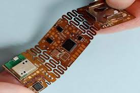
In the realm of modern electronics, high-speed printed circuit boards (PCBs) form the backbone of cutting-edge technologies from 5G communications to artificial intelligence processors. As signal frequencies continue to climb into the multi-gigahertz range, signal attenuation has emerged as one of the most critical challenges facing PCB designers. This paper explores comprehensive strategies to minimize signal attenuation in high-speed PCB designs, covering material selection, transmission line optimization, via design, power integrity considerations, and advanced manufacturing techniques.
Understanding Signal Attenuation in High-Speed PCBs
Signal attenuation in high-speed PCBs refers to the reduction in signal strength as it propagates through transmission lines. This phenomenon becomes increasingly problematic at higher frequencies due to several factors:
Conductor Losses: As frequency increases, current tends to crowd toward the surface of conductors (skin effect), increasing effective resistance.
Dielectric Losses: The PCB substrate material absorbs electromagnetic energy, converting it to heat through molecular dipole rotation.
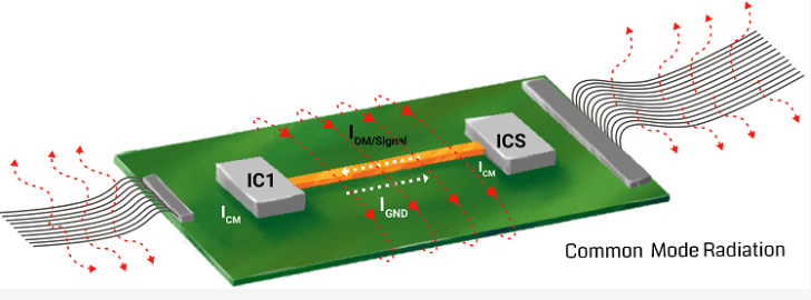
Radiation Losses: High-frequency signals can radiate energy into surrounding space, especially in poorly designed transmission lines.
Reflection Losses: Impedance discontinuities cause signal reflections that effectively reduce transmitted signal power.
The cumulative effect of these losses can severely degrade signal integrity, leading to increased bit error rates, reduced maximum transmission distances, and potential system failures. Let’s examine strategies to mitigate each of these attenuation mechanisms.
1. Material Selection for Minimal Loss
1.1 Low-Loss Dielectric Materials
The choice of PCB substrate material profoundly impacts high-frequency performance. Standard FR-4, while cost-effective, exhibits significant dielectric losses (tan δ ≈ 0.02) at frequencies above 1 GHz. Advanced alternatives include:
- Rogers RO4000 series: With tan δ as low as 0.0027, these ceramic-filled hydrocarbon materials offer excellent high-frequency performance.
- Isola I-Tera MT40: Featuring ultra-low loss (tan δ ≈ 0.0019) and consistent dielectric constant across frequency.
- Nelco N4000-13: A cost-effective mid-range option with tan δ ≈ 0.009.
When selecting materials, consider the trade-off between cost and performance across your operating frequency range.
1.2 Copper Surface Roughness
Standard rolled copper foil exhibits surface roughness that increases conductor losses at high frequencies. Options for improvement include:
- Low-profile copper: Smoother copper surfaces reduce skin effect losses
- Reverse-treated copper: Provides optimal balance between roughness for adhesion and smoothness for conduction
- Electrodeposited copper with additive technology: Can achieve extremely smooth surfaces for critical applications
2. Transmission Line Optimization
2.1 Controlled Impedance Design
Maintaining consistent characteristic impedance along the entire signal path minimizes reflection losses:
- Use field solvers to calculate precise trace dimensions for target impedance
- Account for manufacturing tolerances in your design rules
- Maintain consistent dielectric thickness around critical traces
2.2 Appropriate Transmission Line Geometry
Select the optimal transmission line type for your application:
- Microstrip: Simple to design but more susceptible to external influences
- Stripline: Provides better shielding but requires more layers
- Coplanar waveguide: Offers excellent high-frequency performance with proper grounding
2.3 Trace Width and Thickness Considerations
- Wider traces reduce conductor losses but increase capacitive loading
- Thicker copper (2 oz or more) helps but may require wider traces to maintain impedance
- Balance width and thickness based on your specific loss budget
3. Via Design and Transition Optimization
3.1 Minimizing Via Stubs
Via stubs create impedance discontinuities and resonant structures:
- Use back-drilling to remove unused via portions
- Implement blind or buried vias when possible
- Consider microvia technology for high-density interconnects
3.2 Via Anti-Pad Optimization
Proper clearance around vias in reference planes is crucial:
- Larger anti-pads reduce parasitic capacitance but may weaken plane integrity
- Use teardrop-shaped anti-pads for smoother transitions
- Consider via fencing for critical signals
3.3 Via Count Reduction
Each via introduces some loss and discontinuity:
- Route critical signals on single layers when possible
- Use layer transitions only when necessary
- Group necessary vias close together to minimize dispersion
4. Power Integrity Considerations
4.1 Proper Decoupling Strategy
Inadequate power delivery can manifest as signal integrity issues:
- Implement a mixed decoupling approach with bulk, ceramic, and high-frequency capacitors
- Place decoupling capacitors as close as possible to power pins
- Use appropriate capacitor values for target frequency ranges
4.2 Power Plane Design
- Maintain low-impedance power delivery networks
- Use multiple thin dielectric layers between power and ground
- Implement proper plane stitching via stitching vias
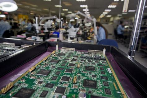
5. Advanced Manufacturing Considerations
5.1 Impedance Control During Fabrication
Work closely with your PCB manufacturer to:
- Specify impedance testing requirements
- Understand their process capabilities and tolerances
- Request impedance test reports for critical traces
5.2 Surface Finishes
The final surface finish affects high-frequency performance:
- ENIG (Electroless Nickel Immersion Gold): Good overall performance
- Immersion Silver: Excellent high-frequency characteristics
- OSP (Organic Solderability Preservative): Simple but may increase connector resistance
5.3 Stackup Design Optimization
A well-planned layer stackup can significantly reduce losses:
- Place critical signals adjacent to solid reference planes
- Balance the stackup to prevent warpage
- Consider hybrid stackups with different materials for different purposes
6. Simulation and Verification
6.1 Pre-Layout Simulation
Use electromagnetic field solvers to:
- Predict insertion loss before fabrication
- Optimize trace geometries and routing
- Identify potential resonance issues
6.2 Post-Layout Analysis
Perform comprehensive analysis including:
- Full-wave 3D EM simulation of critical paths
- Time-domain reflectometry (TDR) analysis
- Power integrity co-simulation
6.3 Measurement Correlation
- Perform vector network analyzer (VNA) measurements on prototypes
- Correlate measurements with simulations
- Iterate design based on empirical results
Conclusion
Minimizing signal attenuation in high-speed PCB design requires a holistic approach addressing materials, geometry, interconnects, power delivery, and manufacturing processes. As signal frequencies continue to rise with emerging technologies, designers must master these techniques to ensure reliable system performance. By implementing the strategies outlined in this paper—from careful material selection to rigorous simulation and verification—engineers can significantly reduce signal attenuation and push the boundaries of high-speed digital design.
The future of high-speed PCB design will likely bring new challenges and solutions, including more sophisticated materials, 3D integration techniques, and AI-assisted design optimization. Staying abreast of these developments while mastering fundamental signal integrity principles will remain essential for success in this demanding field.