Streamline Flexible PCB Prototype Design in 5 Steps
Key Takeaways
When approaching flexible PCB prototype development, understanding core principles ensures you avoid common pitfalls. Start by optimizing layouts for dynamic bending requirements – this means balancing trace routing with mechanical stress points. Partnering with experienced PCB manufacturing companies helps align your design with industry-standard tolerances, particularly when working with polyimide or PET substrates.
Next, consider PCB manufacturing cost drivers early in the process. For example:
| Design Factor | Cost Impact | Mitigation Strategy |
|---|---|---|
| Layer Count | High | Simplify stack-up where possible |
| Material Choice | Moderate | Use standard substrates unless high-temperature performance is critical |
| Tolerances | Variable | Specify tighter tolerances only for critical areas |
Ensuring design manufacturability from the outset reduces revisions, accelerates timelines, and keeps your PCB manufacturing business case viable. Integrate feedback loops with fabricators to validate flex-rigid transitions or adhesive selections. Finally, leverage advanced simulation tools to pre-test designs under real-world conditions, minimizing prototyping cycles. By aligning these steps, you create a workflow that balances speed, reliability, and cost-efficiency – essential for succeeding in competitive markets.

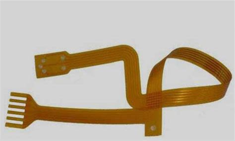
Optimize Layouts for PCB Flexibility
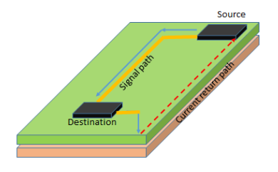
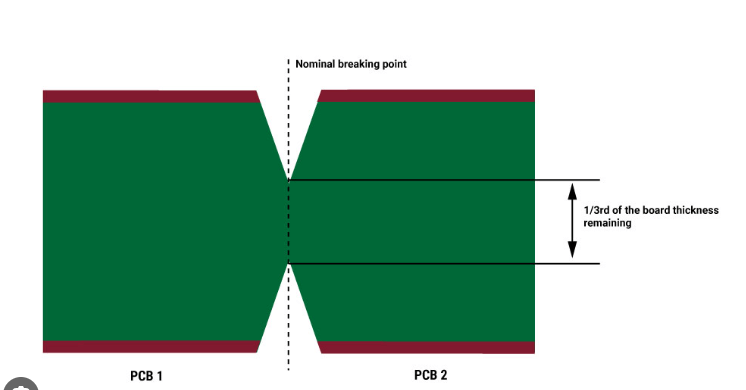
When designing flexible PCB prototypes, your layout strategy directly impacts both functionality and PCB manufacturing cost. Start by analyzing bend regions to minimize stress on copper traces—use curved corners instead of sharp angles to reduce fatigue. Dynamic stress areas require wider traces or additional shielding to maintain signal integrity during repeated flexing. Collaborate early with PCB manufacturing companies to align your design with their fabrication capabilities, ensuring features like staggered vias or teardrop connections meet their process tolerances.
Prioritize component placement in static zones, keeping heavy or rigid elements away from foldable sections. This avoids mechanical strain and simplifies assembly workflows for PCB manufacturing business partners. Utilize simulation tools to validate bend radii and material behavior under real-world conditions—this preemptive step reduces iterations and accelerates time-to-market.
Finally, optimize layer stacking for flexibility and durability. Thin polyimide substrates paired with rolled annealed copper improve bend performance without compromising conductivity. By integrating these practices, you create designs that balance technical requirements with PCB manufacturing realities, lowering risks of delays or costly redesigns.
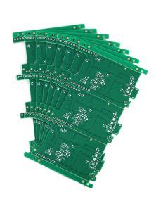
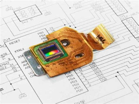
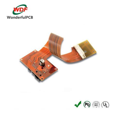
Select Materials for Prototype Durability
When developing flexible PCB prototypes, your material choices directly impact both performance and longevity. Start by evaluating thermal stability and mechanical stress resistance—critical factors for applications requiring repeated bending or exposure to harsh environments. Common substrates like polyimide films offer excellent heat resistance, while adhesive systems must balance flexibility with bond strength.
Collaborate early with PCB manufacturing companies to align material specifications with production capabilities. For instance, ultra-thin copper layers might reduce PCB manufacturing cost but require specialized handling to avoid wrinkles during lamination. Similarly, selecting low-loss dielectrics can improve signal integrity in high-frequency designs but may extend lead times if not readily available.
Consider how material decisions affect the broader PCB manufacturing business workflow. Opting for industry-standard thicknesses (e.g., 1-2 mil polyimide) ensures compatibility with automated assembly lines, reducing rework risks. Validate choices through accelerated life testing to simulate real-world conditions, ensuring your prototype withstands dynamic loads without delamination or cracking.
By prioritizing durable, process-compatible materials, you create a foundation for smoother transitions into scaled production—a strategic step before addressing design manufacturability in the next phase.
Ensure Design Manufacturability Early On
After finalizing your layout and material choices, shift focus to designing with production realities in mind. Engaging PCB manufacturing companies during the initial stages helps identify potential bottlenecks—such as tight tolerances or unconventional geometries—that could inflate PCB manufacturing cost or delay timelines. Use design for manufacturing (DFM) principles to align your prototype with industry-standard fabrication processes, minimizing rework. For example, verify that trace widths, spacing, and bend radii comply with your manufacturer’s capabilities using automated design rule checks (DRCs).
Consider how material choices impact PCB manufacturing business workflows. Flexible circuits requiring specialized adhesives or layered substrates might demand custom tooling, adding complexity. Collaborate with engineers to balance performance needs with cost-effective scalability—like opting for standard polyimide thicknesses instead of bespoke solutions. Early communication also clarifies testing requirements, ensuring prototypes meet both electrical and mechanical validation criteria before mass production.
By addressing manufacturability upfront, you avoid costly mid-process revisions. Simplify assembly by standardizing component footprints or avoiding mixed-technology placements unless absolutely necessary. Remember: a prototype that’s easier to produce accelerates iterations and strengthens partnerships with PCB manufacturing partners, turning theoretical designs into functional products faster.
Accelerate Production With Smart Planning
To compress timelines without sacrificing quality, begin by synchronizing your design process with PCB manufacturing requirements. Proactive collaboration with PCB manufacturing companies during the layout phase helps identify potential bottlenecks—like panelization inefficiencies or material compatibility issues—before they delay production. Use automated design rule checks (DRCs) tailored for flexible circuits to minimize rework, ensuring your files meet exact fabrication specs on the first submission.
Map out milestone-driven schedules that align with your manufacturer’s capacity. For instance, confirm lead times for specialty materials upfront to avoid last-minute substitutions that inflate PCB manufacturing cost. Modern PCB manufacturing business operations often leverage digital twin simulations to validate assembly processes virtually, reducing physical prototyping cycles by up to 40%.
Finally, adopt batch ordering strategies for multiple design iterations. This approach lets you test variations concurrently while maintaining economies of scale. By aligning your workflow with the manufacturer’s production calendar, you transform rigid timelines into adaptive schedules that accelerate time-to-market without overextending budgets.
Implement Cost-Efficient Workflow Strategies
To minimize pcb manufacturing cost while maintaining quality, begin by integrating digital tools like automated design rule checks (DRC) and real-time collaboration platforms. These reduce manual revisions and accelerate feedback loops between your team and pcb manufacturing companies. For instance, using cloud-based software ensures all stakeholders access the latest design iterations, preventing costly miscommunications.
Tip: Request a design-for-manufacturability (DFM) analysis early in the process—many pcb manufacturing business partners offer this service to identify potential cost drivers before prototyping.
Standardizing components across projects simplifies sourcing and lowers bulk material expenses. Work with suppliers to identify high-availability parts that meet your technical requirements, avoiding custom orders that inflate pcb manufacturing timelines and budgets. Additionally, adopt modular design practices to reuse proven circuit blocks, reducing development cycles by up to 30%.
Finally, analyze production data from past projects to spot inefficiencies. Metrics like yield rates and assembly time per unit help refine workflows, ensuring your next prototype aligns with both technical goals and financial constraints. By balancing innovation with practicality, you create a repeatable framework that scales with your pcb manufacturing needs.
Integrate Design and Manufacturing Phases
To achieve seamless PCB manufacturing, bridge the gap between design and production by involving PCB manufacturing companies early in your workflow. Start by sharing your design files with fabrication partners during the initial stages—this allows engineers to flag potential issues like minimum trace widths or bend radius limitations that could inflate PCB manufacturing cost or delay timelines. Use collaborative design tools that align with your manufacturer’s capabilities, ensuring features like stack-up configurations and material choices meet their equipment specifications.
Adopt a “design-for-manufacturability” mindset by running automated checks for solder mask clearances or impedance mismatches. This proactive approach reduces costly revisions and keeps your PCB manufacturing business partnerships efficient. For instance, selecting polyimide substrates over cheaper alternatives might lower long-term risks but requires confirming availability with suppliers. Finally, synchronize prototyping milestones with your manufacturer’s production calendar—this accelerates feedback loops and ensures design tweaks align with their capacity, cutting lead times by up to 30%. By unifying these phases, you turn theoretical designs into functional prototypes without compromising on quality or budget.
Validate Designs Through Rigorous Testing
Before finalizing your flexible PCB prototype, you must subject it to comprehensive testing protocols. Start by simulating real-world operating conditions—expose the design to thermal cycling, mechanical stress, and signal integrity checks to identify weaknesses. Partnering with experienced PCB manufacturing companies ensures access to advanced testing equipment, such as automated optical inspection (AOI) and flying probe testers, which detect microscopic fractures or underperforming connections early.
Integrate failure mode analysis to anticipate potential flaws in high-flex zones or dynamic applications. For instance, validate bend radius limits by replicating repeated folding motions 1.5x beyond expected use to confirm durability. This process not only safeguards performance but also reduces PCB manufacturing cost by preventing post-production redesigns.
While testing, align your criteria with PCB manufacturing business standards to ensure compatibility with production workflows. Document every test iteration meticulously, creating a traceable record for future iterations. By prioritizing rigorous validation, you bridge the gap between design intent and manufacturable reality—a critical step in delivering reliable, cost-effective prototypes that meet both technical and commercial demands.
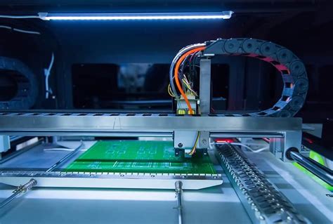
Leverage Advanced Prototyping Technologies
To achieve precision in flexible PCB prototypes, adopt cutting-edge tools like rapid prototyping software and automated simulation platforms. These technologies enable you to visualize PCB manufacturing constraints in real time, minimizing design flaws before production begins. For instance, 3D modeling software identifies mechanical stress points in bend areas, while thermal analysis tools predict performance under extreme conditions. Partnering with experienced PCB manufacturing companies ensures access to advanced laser direct imaging (LDI) systems, which enhance trace accuracy and reduce etching errors by up to 30%.
Integrate design-for-manufacturability (DFM) checks early to align your prototype with factory capabilities, avoiding costly revisions. Modern PCB manufacturing business workflows often combine additive printing and hybrid rigid-flex techniques to accelerate iteration cycles. By leveraging these methods, you can slash PCB manufacturing cost by optimizing material usage and minimizing waste. For high-frequency applications, consider embedded component technologies to shrink board size while maintaining signal integrity.
This approach not only streamlines validation but also bridges the gap between design intent and production reality, ensuring your flexible PCB prototypes meet both functional and budgetary targets.
Conclusion
Perfecting your flexible PCB prototype requires balancing innovation with practical PCB manufacturing realities. By focusing on optimized layouts and material selection, you create designs that meet both technical demands and PCB manufacturing cost constraints. Partnering with experienced PCB manufacturing companies ensures your prototypes align with production capabilities from the start—eliminating costly redesigns and delays.
When refining workflows, consider how design-for-manufacturability principles directly impact your PCB manufacturing business outcomes. Implementing automated verification tools and maintaining open communication with fabrication teams can compress timelines by 30-40%. Remember: every hour saved in prototyping multiplies across production batches.
Finally, validate designs through real-world simulations before committing to full-scale production. This step not only reduces material waste but builds confidence in your prototype’s performance. By integrating these strategies, you transform flexible PCB development from a trial-and-error process into a predictable, cost-controlled workflow—positioning your projects for success in competitive markets.
Frequently Asked Questions
How does flexibility affect PCB manufacturing costs?
Flexible PCB prototypes often incur higher pcb manufacturing cost due to specialized materials and processes. However, working with experienced pcb manufacturing companies can help optimize expenses through design adjustments and bulk material sourcing.
What should I prioritize when selecting a PCB manufacturing business?
Focus on partners with expertise in flexible pcb prototypes, as they’ll ensure design manufacturability and compliance with industry standards. Verify their capabilities in handling advanced materials and rapid prototyping workflows.
How early should I involve manufacturers in my design phase?
Engage pcb manufacturing teams during the layout optimization stage. Early collaboration prevents costly redesigns by aligning your plans with production realities, such as material limitations or assembly constraints.
Can prototyping timelines overlap with final production planning?
Yes. Many pcb manufacturing companies use parallel workflows to accelerate timelines. For instance, validating design aspects like bend radius during prototyping can streamline full-scale production later.
What tools help reduce risks in flexible PCB projects?
Leverage DFM (Design for Manufacturability) software provided by pcb manufacturing partners. These tools flag issues like improper trace spacing or material mismatches before prototyping begins.
Need Expert Support for Your PCB Project?
For tailored solutions in pcb manufacturing business strategies, please click here to connect with specialists who streamline flexible PCB prototyping from design to delivery.