Streamline PCB Production with Gerber File Conversion

Key Takeaways
When preparing Gerber files for PCB manufacturing, understanding their role in the production chain is crucial. These files act as universal blueprints, translating your design into physical circuit boards. For PCB manufacturing companies, precise conversion minimizes errors that could escalate PCB manufacturing cost due to rework or delays. Start by verifying layer alignment in your Gerber output—misaligned copper or solder mask layers can lead to short circuits or incomplete traces.
Adopting industry-standard RS-274X ensures compatibility with most fabrication equipment, streamlining workflows for your PCB manufacturing business. Use automated verification tools to cross-check drill files against layer data, catching discrepancies early. Optimizing layer stack-ups and including clear fabrication notes further reduces ambiguity, accelerating prototype iterations. Remember, even minor oversights in Gerber processing can compound into costly bottlenecks—double-check file integrity before submission. By mastering these techniques, you’ll not only enhance production efficiency but also build stronger partnerships with fabricators through consistent, error-free deliverables.
Gerber File Conversion for Error-Free PCBs
Accurate Gerber file conversion forms the backbone of reliable PCB manufacturing, acting as the digital blueprint that guides fabrication processes. When preparing files for PCB manufacturing companies, you must ensure layer alignment precision and aperture definition clarity to avoid costly rework. Even minor discrepancies—like mismatched drill layers or incomplete copper pours—can escalate PCB manufacturing costs by 15–30% due to material waste and delayed timelines.
To streamline workflows, consider these common Gerber-to-PCB conversion challenges and solutions:
| Error Type | Impact on Production | Preventive Measure |
|---|---|---|
| Missing solder mask layers | Exposed copper risks | Cross-verify layer counts |
| Incorrect aperture sizes | Trace connectivity failures | Use standardized DRC tools |
| Misaligned drill files | Component placement errors | Validate XY coordinates |
Adopting automated verification software reduces human error, ensuring files meet industry-approved guidelines before submission. For PCB manufacturing businesses, this translates to faster prototype iterations and improved client trust. Always confirm that your design software exports RS-274X files—the modern Gerber format—to maintain compatibility with global fabrication standards. By prioritizing meticulous file checks, you safeguard your projects against avoidable setbacks, keeping production timelines and budgets intact.
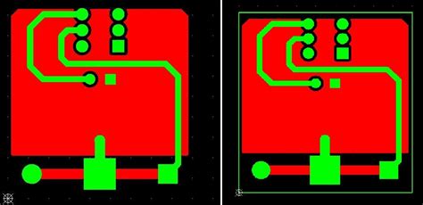
Mastering Layer Alignment in PCB Design
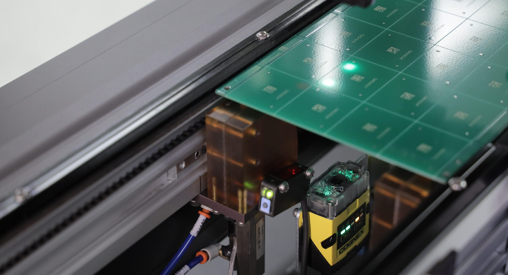
Precise layer alignment is critical when preparing Gerber files for PCB manufacturing, as even minor misalignments can lead to costly errors like short circuits or broken connections. To ensure accuracy, start by verifying your design software’s stack-up configuration—this defines the order and spacing of copper, solder mask, and silkscreen layers. Most PCB manufacturing companies recommend using fiducial markers as alignment references, which act as visual guides for automated assembly equipment.
"Always cross-check layer registration marks in your Gerber files before submission. A 0.1mm offset might seem negligible, but it can escalate PCB manufacturing cost due to rework or scrap."
When exporting Gerber files, confirm that all layers share a common origin point. Tools like CAM software can simulate layer overlaps to identify mismatches early. For multilayer boards, pay extra attention to drill files—misaligned vias or pads can compromise electrical continuity. Tight alignment tolerances (typically ±0.05mm) are non-negotiable for high-density designs, especially in applications like IoT or wearables where space constraints dominate.
Collaborating with PCB manufacturing business partners during the design phase helps align expectations. Many providers offer Design for Manufacturing (DFM) checks to flag alignment risks before production begins. By prioritizing layer synchronization, you reduce prototyping iterations and accelerate time-to-market—a strategic advantage in competitive electronics markets.
Industry-Standard Gerber-to-PCB Techniques
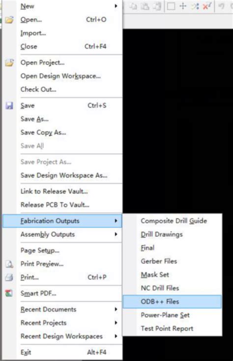
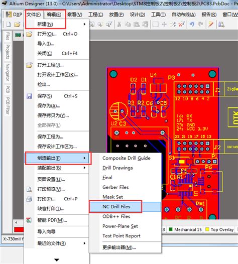
Adopting industry-standard Gerber-to-PCB techniques ensures your design aligns with the rigorous requirements of modern PCB manufacturing. These methods prioritize precision in layer mapping, drill file synchronization, and aperture definitions, minimizing errors that could escalate PCB manufacturing cost or delay timelines. For instance, using RS-274X (Extended Gerber) guarantees accurate data encapsulation, enabling PCB manufacturing companies to interpret your files without ambiguity.
To optimize workflows, verify that copper layers, solder masks, and silkscreens adhere to IPC-2581 or ISO 9001 specifications. Automated tools like DFM (Design for Manufacturability) checks identify mismatches in layer alignment or annular ring widths before production begins. This proactive approach not only reduces rework but also strengthens your PCB manufacturing business by delivering consistent quality.
When executing these standards, ensure your Gerber files include clear layer naming conventions and stack-up details. Many PCB manufacturing companies rely on this metadata to validate designs against their fabrication capabilities. By integrating these practices, you streamline communication with vendors, accelerate prototype approvals, and maintain compliance with global PCB manufacturing benchmarks.
Accelerate Prototyping with Gerber Processing
When preparing files for PCB manufacturing, the precision of your Gerber processing directly impacts prototyping speed and accuracy. By optimizing layer alignment and adhering to industry-standard formats like RS-274X, you eliminate ambiguities that could delay production. Modern PCB manufacturing companies rely on error-free Gerber files to automate fabrication, reducing manual checks and accelerating turnaround times.
To minimize PCB manufacturing cost, ensure your design intent is preserved during conversion. Use stack-up verification tools to cross-check layer order and copper weights, avoiding costly respins. For complex boards, confirm drill files match apertures to prevent misalignment—common pitfalls that inflate expenses in the PCB manufacturing business.
Leverage automated DFM (Design for Manufacturing) checks within Gerber viewers to flag issues like slivers or insufficient clearances before sending files to fabricators. This proactive approach not only streamlines prototyping but also builds trust with partners by demonstrating adherence to PCB manufacturing standards. By refining your Gerber workflow, you transform raw designs into production-ready boards faster, giving your projects a competitive edge.
Efficient PCB Manufacturing via Gerber Files
To achieve efficient PCB manufacturing, you must first understand how Gerber files act as the universal blueprint for fabrication. These files standardize design intent across PCB manufacturing companies, eliminating ambiguities in layer stack-ups, copper traces, and drill patterns. By leveraging automated Gerber processing, you reduce manual interpretation errors that often lead to costly reworks—a critical factor in managing PCB manufacturing cost.
Modern fabrication tools parse Gerber data to optimize material usage and panelization, directly impacting production efficiency. For PCB manufacturing companies, precise layer alignment (RS-274X format) ensures solder masks and silkscreens match component placements flawlessly. This standardized approach minimizes cross-communication delays between design and fabrication teams, accelerating turnaround times—especially vital for prototyping.
When preparing files, verify design rule checks (DRCs) and aperture definitions to prevent mismatches during photoplotting. Tools like Gerber viewers allow you to simulate outputs before submission, catching issues like overlapping pads or incomplete copper pours. This precision directly impacts PCB manufacturing business scalability, as consistent quality builds client trust and reduces waste.
By mastering these techniques, you transform Gerber files from static deliverables into dynamic tools for streamlining workflows—ensuring every production run aligns with industry benchmarks for speed, accuracy, and cost-effectiveness.

Optimizing Gerber Layers for Seamless Production
To ensure PCB manufacturing workflows operate without hiccups, precise organization of Gerber layers is non-negotiable. Start by verifying that layer alignment matches your design intent, as even minor offsets can cascade into costly errors during fabrication. Most PCB manufacturing companies rely on standardized layer-naming conventions (e.g., "Top Copper" or "Bottom Solder Mask") to avoid misinterpretation—double-check these labels to align with your manufacturer’s requirements.
When preparing files, prioritize stack-up clarity by confirming dielectric thicknesses and copper weights are explicitly defined. This not only minimizes back-and-forth revisions but also helps control PCB manufacturing cost by reducing material waste. Tools like Gerber viewers allow you to simulate layer interactions visually, catching potential overlaps or gaps in power planes or signal traces before production begins.
For PCB manufacturing business teams aiming to scale operations, automating layer validation through scripts or CAM software can slash processing time. Integrate industry-approved checks—such as IPC-2581 compatibility—to ensure your Gerber files meet global benchmarks. Remember, optimized layers aren’t just about avoiding errors; they’re about creating a frictionless handoff between design and fabrication, accelerating timelines while maintaining quality.
PCB Quality Assurance Through Gerber Standards
Adhering to Gerber standards ensures your design intent translates accurately into physical boards, minimizing errors that could derail high-volume production. When submitting files to PCB manufacturing companies, standardized Gerber formats (RS-274X) eliminate ambiguity in layer interpretation, preventing costly misalignments or missing features. By defining copper layers, solder masks, and silkscreens with precise layer mapping, you create a universal blueprint that streamlines communication across fabrication teams.
To optimize PCB manufacturing cost, verify that your Gerber files include annotations for critical tolerances and material specifications. Automated checks for aperture definitions or overlapping traces reduce rework risks, which directly impacts both timelines and budgets. For PCB manufacturing business partners, consistency in file formatting accelerates prototyping cycles—ensuring design revisions align with their equipment’s capabilities.
Implementing design rule checks (DRC) before export further strengthens quality assurance. Tools like CAM processors flag discrepancies between your board layout and PCB manufacturing requirements, such as minimum trace spacing or drill hole sizing. This proactive approach not only safeguards against fabrication errors but also builds trust with manufacturers, positioning your projects for repeatable success.
Streamline Prototyping with Gerber Conversion Tips
To accelerate prototyping, start by ensuring your Gerber files adhere to industry-standard specifications recognized by PCB manufacturing companies. Misaligned layers or incomplete data can lead to costly delays, so verify each layer’s alignment using automated validation tools before submission. This step not only reduces PCB manufacturing cost by minimizing rework but also streamlines communication with fabrication partners.
When preparing files, prioritize design rule checks (DRC) to flag potential issues like insufficient clearances or missing solder masks. Many PCB manufacturing workflows rely on precise Gerber formatting, so double-check drill files and copper layers for consistency. For instance, exporting RS-274X files with embedded apertures ensures compatibility with modern equipment, avoiding misinterpretations during production.
Optimizing Gerber layers also involves simplifying complex geometries where possible. Overly intricate designs may require specialized tooling, inflating expenses in the PCB manufacturing business. By balancing detail with manufacturability, you maintain quality while keeping timelines tight. Finally, always request a design-for-manufacturing (DFM) review—a practice adopted by leading suppliers to catch errors early, ensuring your prototypes transition seamlessly to full-scale production.

Conclusion
When implementing Gerber-to-PCB workflows, your ability to adhere to industry-standard protocols directly impacts production efficiency and reliability. By mastering layer alignment and file conversion best practices, you empower PCB manufacturing companies to minimize errors, reduce PCB manufacturing cost, and accelerate time-to-market for prototypes. This precision ensures that every design iteration aligns with automated fabrication systems, eliminating manual adjustments that often lead to delays.
For businesses scaling their PCB manufacturing business, optimizing Gerber files becomes a strategic advantage. Prioritizing validated layer stacks and drill file accuracy not only streamlines prototyping but also builds trust with fabrication partners. As you refine your approach, focus on leveraging software tools that automate verification—this reduces overhead while maintaining compliance with IPC-2581 or RS-274X standards. Ultimately, integrating these practices strengthens your position in competitive markets, where reducing PCB manufacturing cost without compromising quality remains critical for long-term success.
FAQs
How do Gerber files impact pcb manufacturing cost?
Properly formatted Gerber files reduce errors during fabrication, minimizing material waste and rework expenses. PCB manufacturing companies often charge premiums for correcting design flaws, so precise layer alignment and file validation directly lower production costs.
What standards should Gerber files meet for pcb manufacturing business partnerships?
Adhere to IPC-2581 or RS-274X formats, ensuring layer naming conventions and aperture lists are industry-compliant. Most PCB manufacturing providers require these specifications to avoid misinterpretation of copper traces or solder mask details.
Can automated Gerber processing accelerate prototype timelines?
Yes. Advanced CAM software detects mismatched layers or drill conflicts early, allowing PCB manufacturing companies to fast-track prototyping. This automation reduces manual checks by up to 40%, accelerating time-to-market for complex designs.
How do you verify Gerber files before sending them for pcb manufacturing?
Use viewer tools to cross-check layer stack-ups and confirm aperture matches. Many PCB manufacturing firms offer free file audits—take advantage of these services to preemptively resolve issues like missing solder paste layers.
Explore Professional PCB Manufacturing Solutions
For optimized Gerber-to-PCB workflows and cost-effective production, please click here to connect with industry-certified experts.