Streamlined Home PCB Fabrication Techniques Avoiding Etching Pitfalls

Key Takeaways
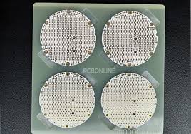
When exploring PCB manufacturing at home, understanding core techniques helps avoid common pitfalls Three primary methods dominate DIY workflows: toner transfer, UV exposure, and CNC milling Each bypasses traditional etching challenges, offering faster turnaround than outsourcing to PCB manufacturing companies
For low-cost prototyping, toner transfer stands out By printing your design onto glossy paper and heat-pressing it onto copper-clad boards, you skip chemical etching However, alignment precision and heat consistency are critical
Tip: Use a laminator instead of an iron for even heat distribution—this reduces toner smudging and improves trace accuracy
UV exposure requires photoresist boards and a UV light source After exposing the board, develop it in a sodium hydroxide solution This method suits complex designs but demands controlled lighting conditions
| Method | Cost (USD) | Tools Required | Best For |
|---|---|---|---|
| Toner Transfer | $20–$50 | Laminator, laser printer | Simple circuits |
| UV Exposure | $60–$120 | UV lamp, photoresist boards | High-detail designs |
| CNC Milling | $300+ | Desktop mill, CAD software | Professional-grade PCBs |
CNC milling eliminates chemicals entirely, carving traces directly onto boards While initial PCB manufacturing cost is higher due to equipment, it’s ideal for repeatable production
Avoiding etching reduces environmental hazards and accelerates prototyping—key for small-scale PCB manufacturing business ventures Troubleshooting common errors (e.g., incomplete traces) often involves adjusting pressure (toner transfer) or exposure time (UV)
“Calibrate tools regularly—even minor misalignments in milling or exposure can derail a project.”
By weighing time, complexity, and PCB manufacturing cost, you’ll identify the optimal approach for your needs Whether prioritizing speed or precision, these methods offer viable alternatives to traditional fabrication
Toner Transfer PCB Technique
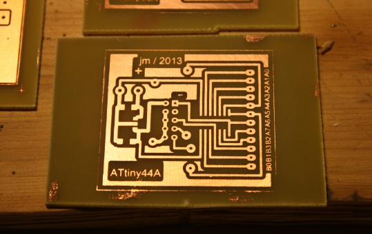
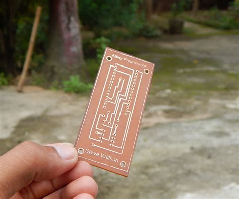
When exploring PCB manufacturing at home, the toner transfer method stands out for its accessibility and minimal equipment requirements This technique allows you to bypass traditional chemical etching by using heat to fuse laser-printed circuit designs onto copper-clad boards To begin, you’ll print your PCB layout onto glossy paper using a laser printer—the toner acts as an etch-resistant mask After trimming the design, you’ll align it precisely on the board and apply heat through a household iron or laminator, transferring the toner pattern onto the copper surface
While this method avoids the hazards of handling etching chemicals, achieving consistent results requires attention to detail Uneven pressure during heating can cause blurred traces, and insufficient heat may leave gaps in the transferred design For multi-layer projects or complex circuits, consider how PCB manufacturing companies use industrial-grade equipment to ensure precision—though their services often come with higher PCB manufacturing costs and lead times
A key advantage of toner transfer lies in its cost-efficiency for prototyping By eliminating the need for UV exposure systems or CNC mills, you reduce upfront investments, making it ideal for hobbyists or small-scale PCB manufacturing business ventures However, you’ll need to factor in material trials: not all paper types release toner cleanly, and some boards may require light sanding for better adhesion
For best results, combine this technique with a ferric chloride alternative (like vinegar-based etchants) if minor corrections are needed This hybrid approach balances speed and control, letting you refine designs without relying entirely on external fabrication services By mastering toner transfer, you gain a foundational skill that bridges DIY experimentation and professional-grade PCB manufacturing workflows
UV Exposure for PCB Creation
When exploring PCB manufacturing techniques suitable for home use, UV exposure stands out as a precision-driven alternative to traditional etching This method relies on photosensitive boards coated with a light-reactive layer, allowing you to transfer circuit patterns using ultraviolet light Start by printing your design onto a transparent film—this acts as a photomask When exposed to UV light, the unshielded areas harden, while the covered sections remain soluble and can be washed away during development
One key advantage lies in avoiding chemical etching altogether, which simplifies waste disposal and reduces safety risks However, success hinges on consistent exposure times and proper alignment of the photomask Even minor gaps or uneven pressure can lead to trace breaks, requiring meticulous setup For multi-layer boards, this method demands precise registration—a challenge some PCB manufacturing companies address with specialized alignment tools in industrial settings
Cost-wise, UV exposure kits are accessible for hobbyists, though initial investments in a UV light source and developer solution may exceed PCB manufacturing cost estimates for small batches Yet, the reusability of films and boards makes it economical for repeated prototyping Unlike outsourcing to PCB manufacturing business providers, this approach eliminates lead times, letting you iterate designs within hours
To optimize results, calibrate exposure duration using test patterns and maintain a dust-free environment—particles on the film can distort traces Post-development, inspect boards under bright light to spot under-etched areas before proceeding to drilling By combining UV exposure with affordable CNC milling for hole drilling, you create a hybrid workflow that balances precision with practicality for home labs
While mastering this technique requires patience, it offers finer line resolution than toner transfer—ideal for dense IC layouts For projects demanding professional-grade tolerances, however, partnering with PCB manufacturing companies remains advisable The goal is to match the method’s capabilities to your project’s complexity, ensuring quality without unnecessary delays or expenses
CNC Milling DIY PCB Guide
When exploring PCB manufacturing at home, CNC milling offers a precise, etching-free alternative to traditional methods Unlike outsourcing to PCB manufacturing companies, this approach puts you in control of the entire process, eliminating delays and reducing PCB manufacturing cost for prototyping To begin, you’ll need a desktop CNC machine, specialized milling bits, and CAD software to convert your circuit design into toolpaths
Start by securing a copper-clad board to the machine’s bed The CNC mill then selectively removes copper traces based on your design, leaving behind clean, isolated pathways Isolation routing, as this technique is called, avoids the messy chemical etching required in conventional PCB manufacturing business workflows One advantage is the ability to handle complex double-layer boards by flipping the substrate and aligning the second side with precision
While commercial PCB manufacturing companies excel at mass production, DIY milling shines for rapid iterations You can test a design, spot errors, and refine traces within hours—a flexibility unmatched by third-party services For optimal results, use a 08mm V-bit for trace isolation and a 32mm end mill for cutting board outlines Dust extraction is critical, as copper particles can interfere with the machine’s accuracy
When comparing costs, consider that a desktop CNC mill requires an upfront investment (typically $500–$2,000), but it pays off if you frequently prototype Unlike outsourcing, which ties PCB manufacturing cost to order volume and lead times, milling lets you produce boards on demand For intricate designs requiring 02mm trace widths, ensure your spindle speed exceeds 24,000 RPM to prevent burring
If you encounter alignment issues during double-sided milling, use fiducial markers in your CAD file to guide repositioning After routing, lightly sand the board with 600-grit paper to remove oxidation and improve solderability While this method demands patience, it bridges the gap between hobbyist experiments and professional-grade PCB manufacturing, offering a middle ground for makers and small-scale developers
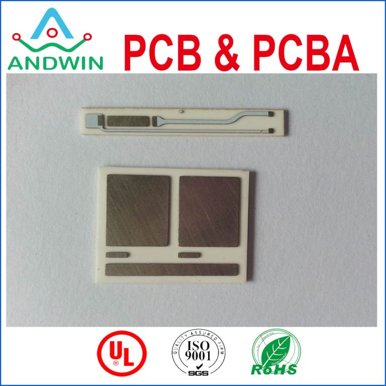
For those tackling high-frequency or multi-layer designs, services like Andwin PCB remain invaluable However, mastering CNC milling empowers you to bypass fabrication delays entirely, turning your workspace into a self-contained prototyping lab
Etching-Free Fabrication Solutions
When building PCB manufacturing projects at home, traditional etching methods often introduce challenges like chemical handling, inconsistent results, and environmental concerns Instead of relying on corrosive ferric chloride or acidic solutions, you can adopt etching-free techniques that streamline production while reducing cost and complexity These approaches bypass the need for hazardous materials, making them safer for hobbyists and small-scale PCB manufacturing businesses alike
For instance, direct milling with a CNC machine allows you to carve copper traces directly onto blank boards, eliminating etching entirely This method offers precision comparable to professional PCB manufacturing companies, though it requires upfront investment in equipment Alternatively, conductive ink printing enables rapid prototyping by drawing circuits with specialized conductive pens—ideal for low-frequency designs or educational purposes While these methods may not match industrial-grade PCB manufacturing cost efficiency for bulk orders, they excel in flexibility for one-off projects or iterative testing
Transitioning to etching-free workflows also reduces dependency on external fabrication timelines You avoid delays caused by chemical processing or outsourcing to third-party services, which is particularly valuable when debugging designs or meeting tight deadlines However, material selection becomes critical: substrates must be compatible with your chosen method, and trace widths may need adjustment to suit non-etching tools By mastering these variables, you’ll build confidence in creating functional boards without the risks and uncertainties of traditional etching—a strategic advantage for anyone exploring PCB manufacturing outside industrial settings
Rapid Prototyping Without Fab Delays
When developing custom circuit boards, waiting weeks for PCB manufacturing companies to deliver prototypes can derail tight timelines This is where in-house rapid prototyping shines, allowing you to bypass traditional fabrication delays while maintaining control over design iterations Unlike outsourced PCB manufacturing, which often involves minimum order quantities and inflated PCB manufacturing costs, DIY methods let you produce functional boards in hours—not days—using tools like desktop CNC mills or direct-print systems
For example, CNC milling eliminates chemical etching entirely by mechanically carving copper traces, making it ideal for testing high-frequency designs or dense layouts By contrast, direct inkjet printing skips both etching and milling, depositing conductive ink onto substrates for ultra-fast revisions These approaches not only accelerate prototyping but also reduce dependency on external PCB manufacturing business workflows, giving you the flexibility to tweak designs between coffee breaks
Critical to success is balancing speed with precision: a poorly calibrated milling bit or misaligned UV exposure unit can waste materials However, modern hobbyist-grade tools now rival industrial equipment in accuracy, with some systems achieving trace widths under 01mm Pairing these with open-source design software creates a closed-loop prototyping environment where you validate concepts before committing to large-scale production
The financial upside is equally compelling While outsourcing a single prototype might cost $50–$200 through conventional PCB manufacturing, DIY setups often break even after 5–10 boards—a viable path for startups or educators managing tight budgets This shift democratizes hardware development, turning garage workshops into micro-factories capable of iterating at the speed of software

Troubleshooting Common PCB Errors
When working with PCB manufacturing at home, you’ll inevitably encounter challenges—even with etching-free methods A recurring issue in techniques like toner transfer is incomplete trace adhesion, often caused by uneven heat application or debris on the copper surface If your design shows broken connections after transferring, recalibrate your laminator’s temperature or clean the board thoroughly with isopropyl alcohol before reapplying the toner For UV exposure setups, over- or underexposure can lead to blurry patterns Use a calibrated light meter to ensure consistent exposure times, and always test-develop a small section first to avoid wasting materials
CNC milling introduces its own quirks, such as depth calibration errors If your machine cuts too shallow, traces may not isolate properly; cutting too deep risks damaging the substrate Regularly check your milling bit’s sharpness and update toolpath settings based on material thickness Short circuits from residual copper strands? A high-powered microscope helps spot hairline fractures or unintended bridges—address them with careful manual trimming or a conductive pen
Even minor design flaws can escalate costs if overlooked For instance, forgetting to invert your design in toner transfer or mirroring errors in UV masks will render the board unusable Software tools like KiCad or Eagle often include design rule checks (DRC) to flag spacing violations or trace width inconsistencies before fabrication While DIY methods bypass delays from PCB manufacturing companies, precision remains critical to avoid costly rework that negates the savings on PCB manufacturing cost
Thermal management is another overlooked factor Overheating during toner transfer can warp thinner substrates, while insufficient heat causes poor adhesion Experiment with time-temperature combinations on scrap materials to find the sweet spot for your setup For those scaling up a PCB manufacturing business, documenting these troubleshooting steps creates a repeatable process, reducing waste and improving yield
By methodically diagnosing these issues, you’ll refine your technique and achieve professional-grade results without relying on external fabrication—keeping your projects on track and within budget
Comparing Home PCB Method Costs
When choosing a PCB manufacturing approach for home use, understanding cost dynamics is crucial While professional PCB manufacturing companies offer standardized pricing, DIY methods vary significantly in upfront investments and recurring expenses Let’s break down the financial implications of popular techniques to help you align your choice with both budget and project requirements
The toner transfer method remains the most budget-friendly option, requiring minimal equipment: a laser printer, iron, and copper-clad board However, hidden costs like specialty transfer paper (or glossy magazine sheets) and consistent failures due to alignment errors can add up For occasional projects, this method keeps PCB manufacturing cost under $50, but frequent use may justify investing in a $200–$400 laminator for better consistency
CNC milling, while precise, demands higher initial spending A reliable desktop mill starts around $1,500, plus bits and software Though it eliminates chemical expenses, wear-and-tear on cutting tools (replacement bits cost $20–$100 each) and time spent on manual calibration contribute to long-term operational costs This makes milling ideal for prototyping complex designs but less economical for single-layer boards compared to outsourcing to PCB manufacturing business services
UV exposure systems strike a middle ground A basic UV light setup costs $80–$200, with photoresist boards and developer chemicals adding $2–$5 per board While cheaper per unit than commercial fabrication for small batches, the learning curve for exposure timing and developing precision can lead to material waste—a critical factor if you’re prioritizing cost predictability
For context, professional PCB manufacturing services typically charge $50–$200 for 5–10 boards, depending on layer count and lead time While this seems steep for one-off projects, economies of scale kick in rapidly; ordering 50+ boards often reduces per-unit costs by 60–70% Comparatively, DIY methods become less viable beyond 10–20 boards due to labor intensity and material exhaustion
Your decision ultimately hinges on volume and urgency Low-quantity prototyping favors home techniques, but for larger batches or multilayer designs, partnering with PCB manufacturing companies ensures better cost efficiency and reliability Always factor in time investment: hours spent troubleshooting DIY errors might offset the perceived savings versus paying a premium for turnkey solutions

Essential Tools for DIY PCB Success
To achieve professional-grade results in home PCB manufacturing, assembling the right toolkit is non-negotiable While commercial PCB manufacturing companies rely on industrial-grade equipment, your workspace can achieve comparable precision with carefully selected tools Start with a high-resolution laser printer for toner transfer methods—its ability to produce crisp, heat-resistant designs on glossy paper is critical for accurate trace replication Pair this with a laminator or heated press to fuse the toner onto copper-clad boards, ensuring adhesion strong enough to survive the developing process
For CNC milling enthusiasts, a desktop router with a carbide micro-bit (02–04 mm) becomes indispensable Look for machines offering ≥001 mm positional accuracy to avoid trace overlaps or breaks If opting for UV exposure, prioritize a UV lightbox with 365–405 nm wavelength settings and a vacuum-sealed exposure frame to eliminate air gaps between the photoresist film and your design transparency
Don’t overlook chemical safety gear—nitrile gloves and fume extractors are mandatory when handling developers or alternative etchants A digital caliper ensures consistent board thickness measurements, while a multimeter with continuity testing helps catch shorts or opens before populating components
While PCB manufacturing cost scales with complexity in professional settings, your DIY setup’s economics hinge on reusability Invest in quality substrates (FR-4 or Rogers materials for RF projects) and modular tooling that adapts to different board sizes For those considering a small-scale PCB manufacturing business, adding a solder paste stencil cutter and reflow oven can bridge the gap between prototyping and low-volume production
Ultimately, your toolkit’s effectiveness depends on pairing hardware with precision software—CAD tools like KiCad or Eagle ensure designs are mill- or etch-ready, while CAM utilities optimize toolpaths and exposure times By mirroring the workflow rigor of commercial fabs, you’ll minimize errors that often plague home fabrication, achieving reliability that rivals outsourced solutions
Conclusion
As you explore etching-free approaches to PCB manufacturing, it becomes clear that modern DIY methods offer viable alternatives to traditional production workflows By mastering techniques like toner transfer, UV exposure, and CNC milling, you gain control over prototyping timelines while sidestepping common chemical-related challenges These methods particularly benefit small-scale projects where collaborating with PCB manufacturing companies might introduce unnecessary delays or elevate PCB manufacturing cost beyond practical limits
The real advantage lies in balancing precision with accessibility—using tools that fit within a compact workspace while achieving results comparable to professional services When evaluating PCB manufacturing business models, notice how these home techniques complement rather than replace industrial processes, serving as a bridge between concept validation and mass production You’ll also develop a deeper understanding of material tolerances and design adjustments, skills that prove invaluable whether you’re troubleshooting a personal project or preparing files for external fabrication
By integrating rapid prototyping into your workflow, you bypass the "waiting game" of outsourced orders, turning revisions into hours rather than days This agility not only accelerates innovation but also refines your ability to anticipate design flaws before scaling up Remember: the goal isn’t to replicate industrial-grade facilities but to cultivate a self-reliant approach that aligns with your specific needs in PCB manufacturing—whether you’re a hobbyist iterating designs or an entrepreneur testing pre-production prototypes
Frequently Asked Questions
What’s the main advantage of home PCB fabrication over using professional PCB manufacturing companies?
Creating PCBs at home allows for rapid prototyping, bypassing lead times from PCB manufacturing services While commercial providers excel in bulk production, DIY methods like toner transfer or milling let you iterate designs in hours, avoiding delays for small-scale projects
How does the cost of DIY methods compare to outsourcing to a PCB manufacturing business?
Home techniques significantly reduce PCB manufacturing cost for prototypes—often under $50 for materials like copper-clad boards and toner sheets However, for complex multi-layer designs or large batches, outsourcing to PCB manufacturing companies becomes more economical due to industrial-grade precision and bulk pricing
Are etching-free methods reliable for high-frequency circuit designs?
UV exposure and CNC milling can achieve traces down to 02mm, suitable for most hobbyist projects For RF or high-speed circuits requiring impedance control, partnering with specialized PCB manufacturing firms ensures tighter tolerances than typical home setups
What safety precautions are critical for DIY PCB manufacturing?
Always wear gloves and goggles when handling UV resins or milling dust If using chemical-free methods, ensure proper ventilation For projects involving etchants (even if avoided here), research local regulations for chemical disposal—a key advantage of etching-free workflows
Can home-fabricated boards match the durability of commercial PCBs?
Properly cured UV solder masks and thorough drilling yield functional boards, but they may lack the thermal resilience or solderability of professionally manufactured ones For mission-critical applications, hybrid workflows—designing at home and outsourcing final production—balance speed and reliability
Ready to Scale Your Prototypes?
For projects requiring industrial-grade precision or larger batches, explore professional solutions at Andwin PCB Click here to request instant quotes and learn how PCB manufacturing companies streamline high-volume production while maintaining cost efficiency