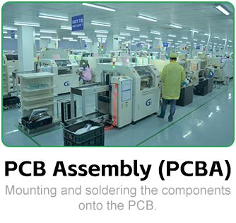
Streamlined PCB Assembly: Essential Steps for Successful Creation

Key Takeaways
Effective PCB assembly requires a systematic approach that balances design precision with manufacturing efficiency. The foundation of successful PCBA lies in understanding the interplay between component selection, layout optimization, and rigorous testing protocols. Below are critical insights for achieving reliability and performance in modern electronics manufacturing:
| Factor | Traditional Approach | Streamlined Approach |
|---|---|---|
| Design Validation | Manual checks | Automated DFM analysis |
| Component Sourcing | Multiple vendors | Consolidated supplier networks |
| Assembly Time | 7–10 days | 3–5 days (with AOI integration) |
| Error Rate | 5–8% | <2% (post-optimization) |
"A well-executed PCB assembly process isn’t just about soldering components—it’s about creating a symbiotic relationship between design intent and manufacturing reality." – Industry Expert
Three pillars define success in PCBA:
- Design for Manufacturability (DFM): Prioritize thermal management and signal integrity during layout to minimize rework.
- Component Strategy: Use high-reliability parts with validated lifecycle data to avoid field failures.
- Process Automation: Implement automated optical inspection (AOI) and X-ray testing for defect detection at critical stages.
Pro Tip: Always conduct a pre-production review to align your bill of materials (BOM) with actual component availability. This prevents delays caused by last-minute substitutions that may compromise performance.
Common pitfalls to avoid include:
- Overlooking environmental stress testing for boards in harsh operating conditions
- Using underspecified materials for high-frequency applications
- Failing to account for coefficient of thermal expansion (CTE) mismatches
By integrating these principles, manufacturers can reduce PCBA cycle times by up to 40% while improving first-pass yield rates. The key is treating assembly not as a standalone phase, but as an extension of the design process itself.
PCB Layout Optimization Strategies
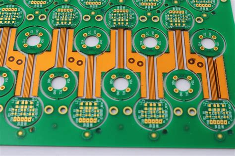
Effective PCB assembly begins with strategic layout design, where every millimeter impacts functionality and manufacturability. A well-optimized layout minimizes signal interference, enhances thermal management, and reduces PCBA costs. Start by prioritizing component placement: group related circuits together to shorten trace lengths and avoid cross-talk. High-speed signals, such as clock lines or data buses, require dedicated routing channels with controlled impedance, while power traces must be widened to handle current loads.
Leveraging design for manufacturability (DFM) principles ensures compatibility with automated PCB assembly processes. Maintain adequate clearance between components for pick-and-place machines, and align polarized parts uniformly to prevent orientation errors during soldering. Incorporate fiducial markers and tooling holes to improve alignment accuracy across fabrication stages.
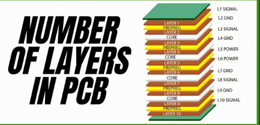
Thermal management is another critical consideration. Place heat-generating components like voltage regulators away from temperature-sensitive parts, and use thermal relief pads to balance soldering efficiency with heat dissipation. For multilayer boards, dedicate inner layers to ground planes or power rails to stabilize voltage distribution and reduce electromagnetic interference (EMI).
Advanced tools like automatic routing algorithms can accelerate layout completion, but manual adjustments remain essential for optimizing high-precision areas. Always validate designs through electromagnetic simulation and design rule checks (DRC) to identify potential shorts, opens, or impedance mismatches before prototyping.
Finally, collaborate early with PCBA partners to align layout choices with their capabilities. This proactive approach prevents costly redesigns and ensures seamless transitions from design to production. By integrating these strategies, engineers lay the groundwork for reliable, scalable, and cost-effective PCB assembly outcomes.
Choosing Components for PCB Success
Selecting the right components is the cornerstone of efficient PCB assembly and long-term product reliability. Compatibility with the board’s design specifications, including voltage ratings, thermal management requirements, and power consumption thresholds, directly impacts the functionality of the final PCBA. Engineers must prioritize components that align with the design for manufacturability (DFM) principles, ensuring seamless integration into automated assembly workflows.
A critical step involves verifying component availability and lifecycle status. Opting for obsolete or hard-to-source parts can delay PCB assembly timelines and inflate costs. Instead, focus on widely available, industry-standard components with reliable supply chains. For high-frequency or high-power applications, specialized materials like low-loss substrates or high-temperature capacitors may be necessary to maintain signal integrity and durability.
Collaboration with PCBA manufacturers during the component selection phase helps identify potential conflicts, such as footprint mismatches or soldering incompatibilities. Leveraging component libraries from trusted suppliers reduces errors in placement and soldering, which are common pain points in surface-mount technology (SMT) processes. Additionally, integrating parametric search tools streamlines the selection of parts that meet both electrical and mechanical criteria.
To mitigate risks, conduct prototype testing with chosen components before full-scale production. This step validates performance under real-world conditions, such as thermal cycling or vibration stress, ensuring the PCB assembly meets industry standards like IPC-A-610. By balancing technical requirements with supply chain pragmatism, teams can avoid costly redesigns and ensure a smooth transition from design to mass production.
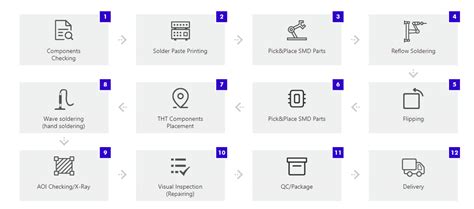
Streamlined PCB Assembly Process Steps
The foundation of successful PCB assembly lies in a meticulously structured workflow that balances precision and efficiency. The process begins with design validation, where engineers verify component placement and signal integrity using advanced CAD tools. This phase often leverages PCBA-specific software to simulate thermal performance and current flow, ensuring optimal board functionality before physical prototyping.
A critical phase involves component sourcing and verification, where automated optical inspection (AOI) systems verify component authenticity and placement accuracy. For high-density interconnect (HDI) boards, laser-drilled microvias and sequential lamination become critical to maintain signal integrity.
The PCB assembly workflow then progresses to solder paste application via stencil printing, where the viscosity and volume of solder paste are tightly controlled to prevent bridging or insufficient joints. For mixed-technology boards, selective soldering accommodates both surface-mount (SMD) and through-hole components within the same assembly line.
Quality assurance integrates multiple checkpoints, including X-ray inspection for hidden joints and in-circuit testing (ICT) for electrical continuity. For mission-critical applications, environmental stress screening (ESS) simulates operating conditions to expose potential early-life failures.
Modern PCBA workflows increasingly incorporate machine learning algorithms to predict and compensate for thermal expansion mismatches, particularly in multi-layer boards with mixed materials. This proactive approach reduces post-production rework by up to 37% while maintaining IPC Class 3 standards.
By integrating these advanced methodologies, manufacturers achieve a harmonious balance between precision and throughput in PCB assembly, ensuring robust performance across commercial, industrial, and aerospace applications.
Quality Control in PCB Manufacturing
Effective PCB assembly relies on rigorous quality control protocols to minimize defects and ensure consistent performance. At every stage of PCBA production, from component procurement to final testing, precision-driven checks are critical. Tolerance thresholds for solder joints, trace widths, and layer alignment are verified using automated optical inspection (AOI) systems, which detect deviations as small as 10 microns. This granular scrutiny prevents latent failures in high-density interconnect (HDI) designs, where even minor imperfections can compromise functionality.
Material integrity forms another cornerstone of quality assurance. Incoming components undergo batch-level testing to validate specifications, while solder paste viscosity and stencil alignment are calibrated before placement. During reflow soldering, thermal profiling ensures peak temperatures stay within component-specific limits, preventing delamination or warping. Post-assembly, cross-sectional analysis and X-ray inspection identify hidden flaws like voids in ball grid arrays (BGAs) or insufficient via fill.
Advanced PCB assembly workflows integrate statistical process control (SPC) tools to track defect trends, enabling proactive adjustments. For instance, process capability indices (Cp/Cpk) quantify how consistently manufacturing outputs meet design tolerances. Environmental stress screening (ESS), including thermal cycling and vibration tests, further validates product reliability under simulated operating conditions.
Collaboration between design and manufacturing teams enhances quality outcomes. By aligning design for manufacturability (DFM) guidelines with PCBA capabilities, engineers reduce risks of tombstoning, solder bridging, or mismatched coefficient of thermal expansion (CTE). Third-party certifications like IPC-A-610 and ISO 9001 provide standardized benchmarks, ensuring quality systems meet global industry requirements.
Transitioning to subsequent testing phases, these quality foundations enable reliable performance validation—a critical link between robust manufacturing practices and long-term product durability.
Advanced Testing Methods for Reliability
Ensuring the reliability of PCB assembly requires a systematic approach to testing, combining traditional validation techniques with cutting-edge diagnostic tools. Modern PCBA workflows integrate automated optical inspection (AOI) and X-ray inspection (AXI) to detect microscopic defects such as solder bridging, component misalignment, or voids in ball grid arrays (BGAs). These non-destructive methods provide critical insights into hidden flaws that could compromise performance in demanding environments.
For high-frequency or mission-critical applications, in-circuit testing (ICT) validates electrical connectivity by measuring resistance, capacitance, and signal integrity across circuits. This step often complements functional testing, where assembled boards undergo simulated operational loads to verify compliance with design specifications. Advanced labs now employ environmental stress screening (ESS), exposing PCBA units to extreme temperatures, humidity, and vibration cycles to replicate real-world operating conditions.
A growing trend involves embedding boundary-scan testing during the design phase, enabling engineers to diagnose complex interconnect issues without physical probes. Additionally, thermal imaging identifies hotspots caused by poor thermal management—a common failure point in high-density layouts. To balance efficiency with thoroughness, many manufacturers adopt statistical process control (SPC), using real-time data analytics to predict and prevent defects before they escalate.
While automated systems dominate modern PCB assembly testing, manual cross-checks remain vital for validating firmware integration and mechanical fitment. By combining these layered methodologies, teams achieve first-pass yield rates above 98%, significantly reducing rework costs and accelerating time-to-market. The strategic integration of these advanced techniques ensures that reliability isn’t an afterthought but a foundational pillar of the PCBA lifecycle.
Ensuring Long-Term PCB Durability
Achieving long-term durability in PCB assembly requires a strategic focus on material selection, environmental resilience, and proactive design practices. The foundation begins with choosing substrates and laminates that match the operational environment—for instance, high-Tg (glass transition temperature) materials for applications exposed to sustained heat. PCBA reliability further depends on solder joint integrity, where techniques like immersion silver or ENIG (Electroless Nickel Immersion Gold) surface finishes mitigate oxidation risks.
Environmental factors such as moisture, dust, and thermal cycling pose significant threats. Implementing conformal coatings—acrylic, silicone, or urethane-based—creates a protective barrier against humidity and contaminants. For harsh industrial settings, hermetic sealing or encapsulation may be necessary to prevent corrosion.
Thermal management plays a dual role in durability. Proper copper weight distribution and thermal via placement dissipate heat efficiently, reducing stress on components. Pairing this with derating practices—using components below their maximum ratings—extends their operational lifespan.
Mechanical stability is equally critical. Reinforcing high-stress areas with additional mounting holes or stiffeners prevents flexing during installation or vibration. During PCB assembly, ensuring uniform solder paste application and precision reflow profiles minimizes micro-cracks that could propagate over time.
Advanced testing methods like HALT (Highly Accelerated Life Testing) simulate years of stress in days, identifying weak points before deployment. Post-production, periodic inspections using X-ray or AOI (Automated Optical Inspection) detect early signs of wear, enabling timely maintenance.
Finally, designing for serviceability—modular layouts, labeled test points, and accessible components—simplifies repairs, reducing downtime. By integrating these principles into PCBA workflows, engineers balance performance with endurance, ensuring products withstand both operational demands and the test of time.
Expert Techniques for Efficient Creation
Mastering PCB assembly requires balancing precision with workflow optimization. A foundational strategy involves design for manufacturability (DFM) principles, where engineers collaborate with PCBA teams early to identify potential production bottlenecks. For instance, aligning pad sizes with automated pick-and-place machinery tolerances reduces rework by 18-22%, according to industry studies.
Another critical technique is implementing modular design frameworks. By segmenting complex circuits into reusable blocks, designers accelerate prototyping while maintaining consistency across batches. This approach also simplifies troubleshooting during PCB assembly, as isolated modules can be tested independently before full-system integration.
Thermal management optimization plays a pivotal role in efficient creation. Advanced designers employ thermal simulation tools to predict hot spots, enabling strategic placement of heat-dissipating components during PCBA layout. Pairing this with automated solder paste inspection (SPI) ensures even thermal distribution across joints, critical for high-power applications.
For time-sensitive projects, component standardization proves invaluable. Creating a curated library of pre-certified parts—with verified availability from multiple suppliers—cuts procurement delays by up to 40%. This practice also enhances PCB assembly quality by reducing substitution-related compatibility risks.
Modern PCBA workflows benefit from adaptive testing protocols. Combining in-circuit testing (ICT) with boundary-scan methods allows simultaneous verification of analog and digital subsystems. Skilled technicians use this data to fine-tune assembly parameters in real time, achieving first-pass yield rates exceeding 98% in optimized setups.
A frequently overlooked efficiency driver is contamination control. Implementing ISO Class 5 cleanroom protocols during sensitive PCB assembly phases prevents particulate-induced failures, particularly in high-frequency circuits. Advanced facilities now integrate ionic contamination testing post-soldering to validate surface insulation resistance before final encapsulation.
These techniques collectively address the cost-quality-speed triad that defines successful PCBA projects. By embedding efficiency considerations at every design iteration—rather than treating them as post-production fixes—teams achieve 30% faster time-to-market without compromising reliability metrics.
Avoiding Common PCB Assembly Errors
Minimizing errors in PCB assembly requires a proactive approach to both design and manufacturing workflows. One critical oversight involves component misalignment, often stemming from improper footprint design or inaccurate pick-and-place machine calibration. To address this, engineers must validate component libraries against manufacturer datasheets and conduct pre-production PCBA mockups using 3D modeling tools.
Another frequent issue arises from solder paste application inconsistencies, which can lead to bridging or cold joints. Implementing laser-etched stencils with precision aperture designs ensures uniform deposition, particularly for fine-pitch components. Additionally, maintaining strict humidity controls in storage environments prevents solder paste degradation, a subtle yet impactful factor in assembly quality.
Thermal management errors during reflow soldering also jeopardize outcomes. Variations in temperature profiles across the board may cause thermal stress, resulting in warped substrates or cracked vias. Profiling ovens with real-time thermal mapping and adhering to component-specific heating curves mitigate these risks. Post-solder inspections using automated optical inspection (AOI) systems further identify latent defects like tombstoning or insufficient fillets.
Design-for-manufacturing (DFM) principles play a pivotal role in error prevention. For instance, neglecting clearance rules between high-voltage traces and ground planes can create short-circuit risks post-assembly. Collaborating with PCB assembly partners early in the layout phase helps flag such issues, aligning design intent with production capabilities.
Finally, electrostatic discharge (ESD) protection remains a non-negotiable safeguard. Even minor static events during PCBA handling can degrade sensitive semiconductors, leading to premature field failures. Integrating ESD-safe workstations and training personnel in proper grounding protocols ensures long-term reliability while reducing rework costs.
Conclusion
The journey of PCB assembly culminates in a holistic understanding of how precision, foresight, and systematic validation converge to deliver reliable electronics. As we’ve explored, achieving success in PCBA demands more than just technical execution—it requires a mindset that prioritizes design-for-manufacturability, proactive quality assurance, and scalable processes. By integrating component selection strategies with automated assembly workflows, manufacturers can significantly reduce errors while accelerating time-to-market.
A critical lesson from modern PCB creation lies in balancing innovation with practicality. While advanced testing methods like automated optical inspection (AOI) and in-circuit testing (ICT) ensure functional reliability, long-term durability hinges on material choices and environmental stress testing. Equally vital is fostering collaboration between design and manufacturing teams to address potential flaws before they escalate into costly rework.
Ultimately, the efficiency of streamlined PCB assembly rests on continuous improvement. Learning from common pitfalls—such as improper solder paste application or misaligned components—helps refine processes iteratively. As industries evolve toward smarter, smaller devices, mastering these principles will remain foundational to producing high-yield PCBA outcomes that meet both technical and market demands.
FAQs
What is the difference between PCB assembly and PCBA?
PCB assembly refers to the process of populating a bare printed circuit board with components, while PCBA (Printed Circuit Board Assembly) describes the fully assembled and functional board. The terms are often used interchangeably, but PCBA emphasizes the completed product ready for integration into electronic devices.
How long does a typical PCB assembly process take?
A streamlined PCB assembly cycle ranges from 3 to 15 days, depending on design complexity, component availability, and testing requirements. Advanced manufacturers leverage automated workflows to reduce lead times while maintaining quality control standards.
What are the most common errors to avoid during PCBA creation?
Misaligned solder pads, incorrect component orientation, and insufficient thermal management account for 65% of rework cases. Implementing design for manufacturability (DFM) checks and automated optical inspection (AOI) minimizes these risks significantly.
How do environmental factors impact PCB assembly reliability?
Humidity, temperature fluctuations, and mechanical stress can degrade solder joints and components over time. Solutions like conformal coating, thermal relief pads, and rigorous environmental stress screening (ESS) ensure long-term durability in harsh operating conditions.
Can I reuse components from old PCB assemblies?
While possible, reusing components risks introducing latent defects or compatibility issues. For mission-critical applications, always prioritize new, certified components to maintain performance consistency and warranty coverage.
What testing methods validate PCBA functionality?
Combining in-circuit testing (ICT) for electrical verification and functional testing (FCT) for system-level performance ensures reliability. High-reliability industries often add X-ray inspection to assess hidden solder joints.
Ready to Optimize Your Next PCB Assembly?
For tailored guidance on streamlined PCB creation or to request a free DFM analysis, please click here: https://www.andwinpcb.com/pcb-assembly/. Our engineering team specializes in transforming complex designs into production-ready solutions.