Streamlined PCB Manufacturing Solutions for Prototyping and Production
Key Takeaways
When evaluating PCB manufacturing partners, it’s critical to prioritize scalability and technical agility. Leading PCB manufacturing companies integrate rapid prototyping with high-volume production capabilities, ensuring seamless transitions from concept validation to market-ready products. By focusing on design for manufacturability (DFM) early in the process, you reduce rework risks, minimize PCB manufacturing cost, and accelerate time-to-market—key factors in staying competitive.
Advanced fabrication technologies, such as laser direct imaging (LDI) and automated optical inspection (AOI), enable precision engineering even for complex multilayer designs. These innovations are particularly valuable for startups and enterprises alike, as they address both prototyping urgency and production consistency. For example, quick-turn services compress lead times to 24–48 hours for prototypes, while bulk orders benefit from economies of scale without compromising quality.
Certified processes—including ISO 9001 and IPC Class 3 standards—ensure reliability across applications, from consumer electronics to aerospace systems. This certification framework not only safeguards against defects but also aligns with global compliance requirements, a non-negotiable for regulated industries.
Cost optimization in the PCB manufacturing business involves balancing material selection, layer count, and panel utilization. Partnering with manufacturers that offer real-time DFM feedback helps identify cost drivers early, such as unnecessary via-in-pad designs or oversized solder masks. Additionally, flexible pricing models—like tiered volume discounts—allow you to align expenses with project milestones.
Finally, quality assurance protocols, such as electrical testing and thermal stress simulations, validate board performance under extreme conditions. By leveraging these practices, you mitigate field failure risks and ensure long-term product viability. Whether scaling a prototype or refining a mature product line, the right PCB manufacturing strategy turns technical constraints into innovation opportunities.
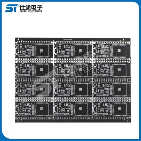
Rapid PCB Prototyping to Bulk Production
When developing electronic products, bridging the gap between prototype validation and full-scale manufacturing requires a seamless transition supported by PCB manufacturing expertise. Modern PCB manufacturing companies leverage advanced workflows to accommodate both low-volume prototyping and high-volume production within unified processes. This dual capability ensures design iterations can be tested rapidly without compromising the scalability needed for market-ready solutions.
For prototyping, agile fabrication techniques like direct imaging and laser drilling enable PCB manufacturing teams to deliver functional boards in as few as 24–48 hours. These quick-turn services allow engineers to verify circuit performance, thermal management, and mechanical fit before committing to bulk orders. However, optimizing PCB manufacturing cost at this stage hinges on early design-for-manufacturability (DFM) analysis. Partnering with a manufacturer that provides real-time DFM feedback helps identify potential bottlenecks—such as non-standard hole sizes or impedance mismatches—that could inflate expenses during scaling.
As demand grows, transitioning to bulk production demands precise coordination of material sourcing, layer stacking, and panel utilization. Reputable PCB manufacturing business providers maintain certified ISO-9001 and IATF 16949 processes to guarantee consistency across thousands of units. Automated optical inspection (AOI) and flying probe testing further ensure defect rates remain below 0.1%, even under high-throughput conditions.
Whether you’re iterating a prototype or ramping up to 10,000+ units, choosing a manufacturer like Andwin PCBA with end-to-end capabilities ensures continuity. Their integrated approach minimizes logistical delays by housing prototyping, testing, and mass production under one roof. Moreover, volume-based pricing models help balance PCB manufacturing cost without sacrificing quality—critical for startups and established enterprises alike.
By aligning your project with a partner skilled in both rapid prototyping and scalable manufacturing, you reduce time-to-market while maintaining the flexibility to adapt designs as technical or market requirements evolve.
Optimizing DFM for Reliable PCB Manufacturing
To achieve consistent quality in PCB manufacturing, optimizing Design for Manufacturing (DFM) principles is non-negotiable. DFM-driven designs minimize production errors by aligning your board’s layout with the capabilities of PCB manufacturing companies, ensuring manufacturability without compromising performance. This starts with adhering to clear design guidelines—like maintaining proper trace widths, spacing, and pad sizes—to avoid costly reworks or delays.
"A thorough DFM review can reduce PCB manufacturing cost by up to 30%, as it identifies potential bottlenecks early in the design phase," notes a senior engineer at a leading fabrication facility.
When you prioritize DFM, you’re not just streamlining production—you’re future-proofing your PCB manufacturing business. For instance, selecting industry-standard materials (e.g., FR-4 or high-frequency laminates) ensures compatibility with automated assembly processes, while avoiding overly complex via structures reduces the risk of fabrication defects. Advanced PCB manufacturing tools, such as automated DFM checkers, can flag issues like insufficient copper balancing or thermal mismatches before prototypes are ordered.
Transitioning from design to production becomes smoother when you collaborate closely with your manufacturer. Share detailed Gerber files, material specifications, and testing requirements upfront to align expectations. Many PCB manufacturing companies offer pre-production DFM analysis as part of their service, which helps refine designs for scalability and reliability. By addressing these factors early, you mitigate risks that could escalate costs or timelines during bulk orders.
Finally, consider how DFM impacts long-term sustainability. Designs optimized for panelization, for example, maximize material utilization, directly lowering PCB manufacturing cost per unit. Pairing this with standardized component footprints ensures smoother assembly, reducing the likelihood of defects in high-volume runs. In a competitive PCB manufacturing business, these optimizations aren’t just technical tweaks—they’re strategic advantages that enhance both product quality and profitability.
Certified Processes for Precision PCB Assembly
When partnering with PCB manufacturing companies, the adherence to certified processes becomes a cornerstone for ensuring product reliability. Modern PCB manufacturing relies on stringent quality frameworks, such as ISO 9001, IPC-A-610, and UL certifications, which govern everything from material selection to final inspection. These standards eliminate variability, ensuring that every board—whether a prototype or a high-volume order—meets exact design specifications.
A critical advantage of certified workflows is their impact on PCB manufacturing cost. While some assume rigorous compliance increases expenses, standardized processes actually reduce waste and rework. For example, automated optical inspection (AOI) and X-ray testing catch defects early, preventing costly failures in later stages. Consider the comparison below:
| Process Stage | Certified Workflow | Uncertified Workflow |
|---|---|---|
| Quality Control | 3-tier inspection protocols | Single visual check |
| Turnaround Time | Predictable timelines | Frequent delays |
| Defect Rate | <0.1% | 2-5% |
| Compliance Assurance | Full traceability | Limited documentation |
For businesses scaling their PCB manufacturing business, certified processes also simplify scalability. Manufacturers with integrated ERP systems streamline order tracking, material procurement, and cross-functional collaboration, enabling seamless transitions from prototyping to mass production. This is particularly vital for industries like aerospace or medical devices, where precision-driven outcomes are non-negotiable.
Moreover, certified PCB manufacturing prioritizes design for manufacturability (DFM) feedback loops. By analyzing your design files against production capabilities upfront, manufacturers identify potential bottlenecks—such as inadequate trace spacing or improper via placement—before fabrication begins. This proactive approach minimizes redesign cycles and accelerates time-to-market.
Ultimately, choosing a partner with certified processes isn’t just about compliance; it’s about aligning your project with proven methodologies that mitigate risk and enhance performance. Whether optimizing PCB manufacturing cost or ensuring repeatability across batches, these frameworks provide the foundation for boards that perform flawlessly under demanding conditions.
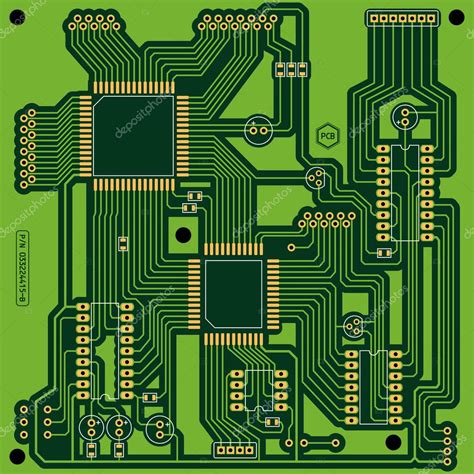
Advanced PCB Fabrication Technologies Explained
Modern PCB manufacturing relies on cutting-edge technologies that balance precision, speed, and scalability. At the core of advanced fabrication methods lies laser direct imaging (LDI), which replaces traditional photomasks to achieve micron-level accuracy in circuit patterning. This approach reduces pcb manufacturing cost by eliminating tooling expenses and minimizing material waste—a critical advantage for both prototyping and high-volume production.
Another critical innovation is automated optical inspection (AOI), integrated seamlessly into workflows by leading pcb manufacturing companies. These systems scan boards at multiple stages, catching defects like micro-shorts or misalignments early in the process. When combined with high-density interconnect (HDI) techniques—enabling complex multilayer designs—these technologies ensure your boards meet the demands of compact, high-performance electronics.
For businesses prioritizing rapid iteration, additive manufacturing methods are transforming the pcb manufacturing business. Semi-additive processes deposit copper only where needed, reducing chemical usage and etching time. This not only accelerates turnaround but aligns with sustainable practices—a growing differentiator in competitive markets.
When evaluating pcb manufacturing cost, consider how advanced panelization software optimizes material utilization. By nesting multiple board designs into single panels, manufacturers reduce raw material consumption by up to 20%, passing savings to clients without compromising quality. Leading firms further leverage IoT-enabled equipment monitoring to predict maintenance needs, ensuring uninterrupted production cycles.
These advancements directly address the thermal management and signal integrity challenges in modern PCBs. Techniques like embedded component packaging and low-loss dielectric materials are becoming standard in high-frequency applications, enabling designs that outperform traditional FR-4 boards. By integrating these technologies, pcb manufacturing companies deliver boards capable of supporting 5G networks, AI processors, and aerospace-grade reliability.
The shift toward industry 4.0 practices in fabrication facilities ensures traceability across every production batch. Real-time data analytics track parameters from copper plating thickness to solder mask viscosity, creating audit trails that simplify compliance with ISO and IPC standards—a non-negotiable for medical or automotive applications.
As you navigate partnerships with pcb manufacturing providers, prioritize those investing in adaptive impedance control and 3D printing for RF components. These emerging technologies future-proof your supply chain, ensuring your products evolve alongside advancing electronic architectures.
Scalable Solutions for Electronics Production Needs
When scaling your electronics projects from prototype to mass production, partnering with the right PCB manufacturing companies becomes critical. These providers specialize in adapting their processes to accommodate fluctuating order volumes without compromising quality—whether you’re testing 10 units or ramping up to 10,000. A key advantage lies in their ability to optimize PCB manufacturing cost structures through economies of scale, ensuring per-unit expenses decrease as your demand grows. This cost efficiency is particularly vital for startups balancing tight budgets with aggressive growth timelines.
Leading PCB manufacturing firms achieve scalability by integrating modular production systems. These systems allow seamless transitions between low-volume, high-mix prototyping and high-volume runs—ideal for industries like IoT or automotive electronics, where design iterations often precede large orders. Advanced manufacturers also employ dynamic material procurement strategies, securing component inventories aligned with your project’s lifecycle stage. For businesses managing seasonal demand spikes, such flexibility prevents overstocking while maintaining rapid turnaround times.
The PCB manufacturing business model thrives on customization. Reputable providers work backward from your technical requirements, applying design-for-manufacturability (DFM) principles to eliminate production bottlenecks before tooling begins. This proactive approach minimizes redesign costs and accelerates time-to-market—a competitive edge when launching products in fast-moving sectors. Additionally, certified manufacturers leverage automated optical inspection (AOI) and real-time yield monitoring to maintain consistency across batches, even at peak capacity.
Scalability extends beyond pure production volume. Forward-thinking partners offer value-added services like warehousing, kitting, and just-in-time delivery to simplify supply chain logistics. By aligning their capabilities with your growth trajectory, PCB manufacturing experts transform operational complexity into strategic advantage, letting you focus on innovation rather than infrastructure constraints.
Quality Assurance in PCB Manufacturing Standards
When selecting PCB manufacturing companies, understanding their approach to quality assurance (QA) is critical for ensuring your boards meet both functional and regulatory requirements. Modern PCB manufacturing relies on a multi-layered QA framework that begins with design validation and extends through every production phase. Leading providers implement IPC-A-600 and ISO 9001 standards to govern material selection, traceability, and process controls, minimizing defects that could escalate PCB manufacturing cost over time.
A robust QA system integrates automated optical inspection (AOI) and X-ray testing to detect micro-cracks, solder voids, or misalignments invisible to the naked eye. For high-frequency or high-density designs, impedance testing ensures signal integrity, while environmental stress screening (ESS) validates performance under extreme temperatures or humidity. These protocols not only reduce rework expenses but also protect your PCB manufacturing business from costly recalls or compliance penalties.
Cost-effective quality management hinges on design-for-manufacturability (DFM) collaboration. By analyzing your design files pre-production, manufacturers can flag potential issues like insufficient copper balancing or unrealistic tolerance thresholds. This proactive alignment between engineering and production teams optimizes yield rates, directly influencing PCB manufacturing cost efficiency without compromising reliability.
Material traceability has become a cornerstone of QA, particularly for aerospace or medical applications. Reputable PCB manufacturing companies maintain batch-level documentation for substrates, laminates, and finishes, enabling rapid root-cause analysis if anomalies emerge. Advanced facilities now employ machine learning algorithms to predict equipment wear or process drift, transforming QA from a reactive checkpoint into a predictive safeguard.
As global supply chains grow more complex, verifying your manufacturer’s counterfeit component prevention measures is equally vital. Certified partners utilize authorized distributors and component authentication technologies to eliminate the risks of substandard materials entering your production stream. This diligence ensures your PCB manufacturing business delivers products that consistently meet lifecycle expectations, even in mission-critical deployments.
By prioritizing these QA dimensions, you create a partnership model where quality becomes a shared KPI rather than an inspection hurdle. The result? Boards that perform as engineered, timelines that hold firm, and costs that align with projected budgets—cornerstones for scaling electronics innovation sustainably.
Accelerating Innovation Through Quick-Turn PCB Services
In today’s fast-paced electronics landscape, speed-to-market often dictates competitive advantage. PCB manufacturing companies specializing in quick-turn services enable you to compress development cycles by delivering functional prototypes within days, not weeks. This rapid iteration capability allows engineering teams to validate designs, identify flaws early, and refine product performance without derailing project timelines. By integrating design-for-manufacturability (DFM) feedback during prototyping, these services ensure your boards align with production realities from the first iteration, reducing costly redesigns later.
The PCB manufacturing cost implications of traditional lead times can strain budgets, especially when delays cascade into missed market windows. Quick-turn providers mitigate this by combining advanced fabrication technologies—like laser direct imaging and automated optical inspection—with streamlined workflows. This approach maintains precision while accelerating turnaround, whether you’re ordering 10 prototypes or scaling to 10,000 units. For startups and enterprises alike, this agility transforms how you approach R&D, turning months-long waits into mere days of focused development.
However, speed alone isn’t enough. Leading PCB manufacturing business models prioritize transparency, offering real-time order tracking and proactive communication. This ensures you’re never left guessing about production milestones, even when operating on tight schedules. Additionally, by leveraging economies of scale and optimized material sourcing, these providers balance accelerated timelines with cost efficiency, making rapid iterations financially viable for projects of all sizes.
By partnering with PCB manufacturing experts who specialize in quick-turn solutions, you gain more than just faster boards—you unlock the flexibility to experiment, pivot, and innovate with confidence. This agility is critical when developing cutting-edge IoT devices, automotive systems, or medical equipment, where even minor design improvements can redefine product success. As demand for smarter, smaller electronics grows, the ability to rapidly translate ideas into functional hardware becomes a cornerstone of modern engineering strategy.
Cost-Effective PCB Production Strategies Unveiled
Achieving cost efficiency in PCB manufacturing requires balancing quality, speed, and scalability. Leading PCB manufacturing companies employ strategic design optimizations, such as design for manufacturability (DFM), to minimize material waste and reduce PCB manufacturing cost from the outset. By refining layouts to standard panel sizes and leveraging automated routing, you can avoid unnecessary complexities that inflate expenses without compromising performance.
Material selection plays a pivotal role. Opting for cost-effective substrates like FR-4 for non-critical layers, while reserving high-frequency materials only for signal-critical areas, ensures your PCB manufacturing business meets budgetary constraints. Partnering with suppliers who offer volume pricing tiers further reduces per-unit costs, especially when scaling from prototyping to full production.
Advanced panelization techniques, such as nested arrays or step-and-repeat layouts, maximize material utilization during fabrication. This approach is particularly impactful for high-volume orders, where even marginal savings per board compound significantly. Additionally, adopting lean manufacturing principles—like just-in-time inventory management—minimizes overhead and aligns production timelines with project milestones.
Automated testing protocols, including automated optical inspection (AOI) and electrical testing, prevent costly rework by catching defects early. While these steps add upfront time, they reduce long-term PCB manufacturing cost by ensuring yield rates remain high. For startups or SMEs, collaborating with manufacturers offering shared tooling or pooled orders can unlock economies of scale typically reserved for larger enterprises.
Finally, transparent communication with your PCB manufacturing partner is key. Clarifying tolerances, delivery windows, and acceptable material substitutions upfront avoids mid-process changes that derail budgets. By integrating these strategies, you transform cost-conscious decisions into competitive advantages, ensuring your electronics projects stay financially viable without sacrificing reliability.
Conclusion
When navigating the complexities of PCB manufacturing, your choice of partner can determine not just product quality but the viability of your entire project. Leading PCB manufacturing companies balance technical expertise with operational agility, ensuring designs transition seamlessly from prototyping to full-scale production. By prioritizing DFM optimization early in the process, you mitigate risks related to assembly errors and material waste, directly influencing PCB manufacturing cost while maintaining compliance with industry certifications.
For startups and established enterprises alike, scalability remains critical. A robust PCB manufacturing business model accommodates fluctuating order volumes without compromising turnaround times or precision—whether you require ten prototypes or ten thousand production-grade boards. Advanced fabrication technologies, coupled with real-time supply chain management, empower manufacturers to deliver high-reliability solutions even for applications with stringent thermal or signal integrity requirements.
As you evaluate providers, consider how their certified processes align with your long-term goals. The right partner doesn’t just fulfill specifications but collaborates to refine designs, identify cost-saving opportunities, and future-proof your electronics. This approach becomes particularly valuable when balancing PCB manufacturing cost against performance benchmarks, ensuring every dollar spent translates into measurable value.
Ultimately, the success of your hardware depends on more than technical capability—it hinges on choosing a manufacturer that understands the intersection of innovation, efficiency, and reliability. By leveraging expertise in PCB manufacturing, you position your projects to thrive in competitive markets while maintaining the flexibility to adapt as technologies evolve.
FAQs
How do you choose between different PCB manufacturing companies for prototyping?
When selecting PCB manufacturing partners, evaluate their technical capabilities and lead times for prototypes. Look for suppliers offering DFM optimization to catch design flaws early, which reduces PCB manufacturing cost by minimizing rework.
What factors most impact PCB manufacturing cost in high-volume production?
Material selection, layer count, and surface finishes drive expenses. Established PCB manufacturing businesses leverage economies of scale, while automated processes ensure consistency. Always request breakdowns of tooling, testing, and material fees to compare quotes accurately.
Why is design for manufacturability (DFM) critical in PCB manufacturing?
DFM reviews align your design with production realities, preventing delays. For example, trace spacing or drill hole alignment issues spotted during DFM can avoid 30%+ cost overruns. Partner with PCB manufacturing companies that provide free DFM checks upfront.
How do certifications affect PCB manufacturing quality?
Certifications like ISO 9001 and IPC Class 3 ensure adherence to industry benchmarks. They validate a supplier’s ability to handle high-reliability applications, from medical devices to aerospace systems. Always verify certifications match your product’s requirements.
Can PCB manufacturing services scale from prototypes to bulk orders seamlessly?
Leading providers use unified processes across prototyping and production. This ensures design compatibility and avoids tooling changes. Confirm their maximum monthly capacity and whether they offer inventory management for large-scale PCB manufacturing business needs.
Ready to Optimize Your PCB Project?
Explore tailored PCB manufacturing solutions that balance speed, quality, and cost. For a detailed consultation or instant quote, please click here.


