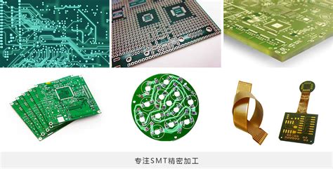
Streamlining Assy PCB Design for Enhanced Performance
Key Takeaways
Optimizing PCB assembly (PCBA) workflows begins with aligning design strategies to core principles that prioritize signal integrity, thermal efficiency, and electromagnetic compatibility. A well-structured assy PCB integrates strategic component placement to minimize noise and crosstalk, particularly in high-speed circuits, while ensuring robust power distribution. Material selection plays a pivotal role—high-Tg substrates and low-loss dielectrics enhance thermal stability and signal performance in demanding environments. Advanced routing techniques, such as differential pair routing and controlled impedance traces, reduce electromagnetic interference (EMI) risks, especially in densely packed layouts. For high-density assemblies, implementing thermal vias, heat sinks, or embedded cooling channels prevents overheating and prolongs component lifespan. Automating repetitive tasks in PCBA design—like footprint generation and design rule checks—accelerates timelines while reducing human error. Rigorous testing protocols, including in-circuit testing (ICT) and automated optical inspection (AOI), validate functionality and reliability before mass production. Looking ahead, innovations such as AI-driven layout optimization and additive manufacturing for multi-layer boards are set to redefine assy PCB efficiency, enabling faster prototyping and smarter integration of mixed-signal components. By balancing these elements, designers can achieve PCB assembly solutions that deliver higher performance, reliability, and scalability across industries.
Foundations of Efficient Assy PCB Design: Core Principles
Efficient PCB assembly (PCBA) design hinges on adhering to core principles that balance functionality, manufacturability, and reliability. At its foundation, a well-structured Assy PCB integrates design for manufacturability (DFM) guidelines to minimize errors during production. This begins with optimizing component placement to reduce signal path lengths, which enhances signal integrity while mitigating electromagnetic interference (EMI). Strategic positioning of high-speed components, power regulators, and decoupling capacitors ensures stable voltage distribution and minimizes noise coupling—critical for high-performance applications.
Material selection is equally vital, as substrate properties directly influence thermal stability and electrical performance. For instance, using high-glass transition temperature (Tg) materials improves resistance to thermal stress in PCBA environments, while low-loss dielectrics support high-frequency signal transmission. Additionally, layer stack-up planning must account for impedance control, especially in mixed-signal designs, to maintain consistent performance across the board.
Advanced routing techniques, such as differential pair routing and via optimization, further reduce EMI risks. Implementing ground planes and shielding structures isolates sensitive circuits, preserving signal clarity. Thermal management strategies, including thermal vias and heatsink integration, prevent hotspots in high-density assemblies, ensuring long-term reliability.
Automation tools streamline workflows by enabling rapid iteration of layout and routing configurations, reducing human error and accelerating time-to-market. By embedding these principles early in the design phase, engineers can achieve robust PCB assembly outcomes that align with performance benchmarks and industry standards.
Strategic Component Placement for Optimal Signal Integrity
Effective PCB assembly relies heavily on strategic component placement to ensure signal integrity and minimize electromagnetic interference (EMI). In PCBA design, the physical arrangement of components directly impacts signal paths, thermal dissipation, and overall system reliability. High-speed digital components, for instance, should be positioned to shorten critical signal traces, reducing latency and cross-talk. Similarly, sensitive analog circuits require isolation from noisy power supplies or switching regulators to prevent distortion.
A key consideration is grouping components by functional blocks. For example, placing decoupling capacitors as close as possible to integrated circuits (ICs) stabilizes power delivery networks (PDNs), mitigating voltage drops and ground bounce. Additionally, orienting components to align with natural signal flow—such as routing clock lines perpendicular to data buses—reduces unintended coupling. Below is a table summarizing placement strategies for common component types:
| Component Type | Placement Strategy | Key Benefit |
|---|---|---|
| High-speed ICs | Near connectors, short trace paths | Minimizes signal attenuation |
| Decoupling capacitors | Adjacent to power pins of ICs | Stabilizes power supply |
| RF modules | Isolated from digital circuits | Reduces EMI interference |
| Thermal-sensitive parts | Away from heat-generating components | Prevents overheating |
Tip: Use simulation tools during the PCB assembly layout phase to model signal behavior and identify potential bottlenecks before prototyping.
Thermal management also plays a role in component placement. High-density PCBA designs often face challenges with heat dissipation. Positioning heat-generating components like voltage regulators near board edges or heat sinks ensures efficient thermal transfer. Conversely, temperature-sensitive parts, such as crystal oscillators, should be shielded from thermal hotspots.
Finally, consider manufacturability. Aligning components uniformly simplifies automated pick-and-place processes, reducing PCB assembly errors. For mixed-signal designs, partitioning analog and digital grounds while maintaining a single reference plane avoids ground loops. By balancing electrical performance with practical PCBA constraints, designers can achieve layouts that are both high-performing and cost-effective.
Material Selection and Its Impact on PCB Performance
The choice of materials in PCB assembly significantly influences the performance, reliability, and longevity of the final product. Substrate materials like FR-4, high-frequency laminates, and metal-core substrates each offer distinct advantages depending on the application’s electrical, thermal, and mechanical demands. For instance, FR-4, a widely used epoxy-based material, provides cost-effectiveness and adequate performance for standard applications, while high-frequency laminates such as Rogers or Teflon-based composites are critical for minimizing signal loss in radio-frequency (RF) or microwave designs. In PCBA environments where thermal management is paramount, metal-core substrates like aluminum or copper improve heat dissipation, reducing the risk of overheating in high-density assemblies. Additionally, the dielectric constant and dissipation factor of the chosen material directly affect signal integrity, particularly in high-speed circuits where impedance control is essential. Advanced thermal interface materials (TIMs) further enhance heat transfer between components and heatsinks, ensuring stable operation under extreme conditions. Engineers must also consider the coefficient of thermal expansion (CTE) to prevent mechanical stress during soldering or thermal cycling, which can lead to delamination or component failure. By aligning material properties with design requirements—such as operating frequency, power density, and environmental factors—teams can optimize PCB assembly workflows to achieve robust, high-performance PCBA solutions without compromising manufacturability or cost-efficiency.
Advanced Routing Techniques to Minimize Electromagnetic Interference
Effective routing is critical in PCB assembly to mitigate electromagnetic interference (EMI), which can degrade signal integrity and overall system performance. A primary strategy involves optimizing differential pair routing to balance signal paths, reducing noise susceptibility. By maintaining consistent trace lengths and spacing, designers ensure synchronized signal propagation, minimizing crosstalk in high-speed PCBA designs. Additionally, employing controlled impedance traces tailored to the board’s material properties helps preserve signal fidelity, especially in RF and mixed-signal applications.
Ground plane optimization plays a pivotal role in EMI suppression. A continuous ground plane beneath signal layers provides a low-impedance return path, shielding sensitive circuits from interference. For multi-layer boards, strategic use of via stitching connects isolated ground regions, preventing ground loops and enhancing EMI dissipation. In dense PCB assembly layouts, 3D routing tools enable precise trace placement around obstacles while adhering to clearance rules, reducing parasitic capacitance and inductive coupling.
Another advanced technique involves segmented power delivery networks (PDNs). By isolating analog and digital power domains, designers minimize noise coupling between subsystems. Transient voltage suppressors and ferrite beads further decouple power rails, stabilizing voltage levels in PCBA environments. To address high-frequency EMI, guard traces or shielding cans are integrated around noise-prone components like oscillators or switching regulators, containing radiated emissions.
Finally, simulation-driven validation using electromagnetic compatibility (EMC) analysis tools allows pre-production testing of routing strategies. By identifying hotspots and refining trace geometries early, teams reduce iterative fixes, accelerating PCB assembly timelines without compromising reliability. These techniques collectively ensure robust EMI management, enabling PCBA designs to meet stringent performance standards in industrial, automotive, and telecommunications applications.
Thermal Management Solutions for High-Density Assemblies
Effective thermal management is critical in PCB assembly (PCBA) for high-density designs, where component proximity and power demands escalate heat generation risks. To mitigate thermal stress, engineers employ advanced strategies such as thermal vias, heat sinks, and thermally conductive substrates. Thermal vias—small plated holes drilled into the board—facilitate heat transfer from high-power components to inner or outer copper layers, dispersing energy efficiently. Pairing these with heat sinks or thermal pads further enhances dissipation, particularly in compact layouts where airflow is restricted.
Material selection also plays a pivotal role. High-performance substrates like metal-core PCBs or ceramics offer superior thermal conductivity compared to traditional FR4, reducing hotspots in high-density assemblies. For instance, embedding copper or aluminum layers within the board structure improves heat spreading, while thermally conductive adhesives ensure secure component bonding without compromising thermal performance.
In PCB assembly workflows, simulation tools are indispensable for predicting thermal behavior. Finite Element Analysis (FEA) models identify potential hotspots early, enabling designers to adjust component placement or optimize copper pour patterns. Additionally, strategic placement of thermal relief pads and balanced power distribution across layers minimizes localized heating, preserving signal integrity and component longevity.
Advanced PCBA techniques, such as integrating embedded cooling channels or phase-change materials, are emerging as solutions for extreme-density applications. These innovations, combined with rigorous testing protocols like infrared thermography, ensure reliable operation under varying load conditions. By harmonizing material science, layout optimization, and predictive modeling, engineers achieve robust thermal management in modern high-density PCB assemblies, safeguarding performance and reliability in demanding environments.
Automating Design Workflows to Accelerate Production Timelines
Automating PCB assembly design workflows is critical to reducing development cycles and ensuring seamless transitions from prototyping to mass production. By leveraging advanced software tools, engineers can automate repetitive tasks such as component placement, signal integrity analysis, and design rule checks (DRC), significantly minimizing human error while accelerating timelines. For instance, autorouting algorithms optimize trace layouts to meet electromagnetic compatibility (EMC) standards, ensuring that PCBA designs adhere to performance and reliability benchmarks. Integrating machine learning models into these workflows further enhances predictive capabilities, enabling real-time adjustments to component positioning or thermal management strategies based on historical data.
Central to this automation is the adoption of unified electronic design automation (EDA) platforms, which synchronize schematic capture, layout design, and simulation phases. These tools enable seamless collaboration between hardware and manufacturing teams, ensuring that PCB assembly requirements—such as solder mask clearances or via placements—are addressed early in the design phase. For high-density assemblies, automated thermal analysis tools identify hotspots and recommend heat dissipation solutions, such as optimized copper pours or component spacing, to prevent performance degradation.
Moreover, automating documentation processes—including bill of materials (BOM) generation and fabrication notes—streamlines communication with PCBA manufacturers, reducing delays caused by manual revisions. By standardizing design templates and libraries for frequently used components, teams can maintain consistency across projects while scaling production efficiently. This approach not only accelerates time-to-market but also ensures that PCB assembly processes align with evolving industry standards, from RoHS compliance to lead-free soldering techniques.
Ultimately, the strategic implementation of automation in PCBA workflows bridges the gap between design innovation and manufacturability, enabling engineers to focus on performance optimization rather than repetitive tasks. As technologies like AI-driven design assistants and cloud-based collaboration tools mature, their integration will further redefine efficiency in PCB assembly ecosystems.
Testing and Validation Protocols for Reliable PCB Functionality
Ensuring the reliability of PCB assembly (PCBA) requires rigorous testing and validation protocols that address both functional performance and long-term durability. These protocols begin with in-circuit testing (ICT), which verifies the electrical connectivity of components and identifies shorts, opens, or incorrect values. For high-density assemblies, automated optical inspection (AOI) complements ICT by detecting soldering defects, misaligned components, or missing parts. Advanced electromagnetic compatibility (EMC) testing is also critical to ensure the design minimizes interference, particularly in applications sensitive to noise.
Environmental stress tests, such as thermal cycling and vibration testing, simulate real-world operating conditions to validate the PCB assembly’s resilience under extreme temperatures or mechanical strain. Additionally, functional testing replicates the end-use scenario to confirm that the PCBA meets all operational requirements. For mission-critical systems, boundary scan testing provides deeper insights into integrated circuits, enabling fault detection in complex, multi-layer designs.
Data-driven validation tools, like signal integrity analysis and power distribution network simulations, further refine the process by identifying potential bottlenecks before physical prototyping. By integrating these protocols early in the PCB assembly workflow, manufacturers reduce iterative redesigns and accelerate time-to-market while maintaining compliance with industry standards. Robust documentation and traceability systems, often enhanced by machine learning algorithms, ensure every PCBA unit adheres to predefined quality benchmarks, ultimately delivering consistent performance across production batches.
Future Trends in Assy PCB Design: Innovations to Watch
The evolution of PCB assembly (PCBA) is being driven by advancements in automation, material science, and design methodologies. One key trend is the integration of AI-driven design tools, which optimize component placement and routing by analyzing vast datasets to predict signal integrity issues and thermal hotspots. These tools enable designers to create high-density layouts while minimizing electromagnetic interference (EMI)—a critical factor for applications in 5G, IoT, and automotive electronics. Another emerging innovation is the use of advanced substrates, such as high-frequency laminates and flexible materials, to enhance performance in compact or wearable devices. Additionally, additive manufacturing techniques are gaining traction, allowing for rapid prototyping of complex PCBA geometries that traditional methods struggle to produce. The rise of modular design frameworks is also streamlining workflows, enabling reusable blocks of circuitry to be integrated seamlessly across projects, reducing development cycles. Sustainability is becoming a priority, with manufacturers adopting eco-friendly materials and processes to minimize waste in PCB assembly. Finally, the adoption of embedded components—such as capacitors and resistors within the board layers—promises to reduce footprint and improve reliability, particularly in mission-critical systems. As these trends converge, the future of Assy PCB design will prioritize scalability, energy efficiency, and fault tolerance, ensuring next-generation electronics meet escalating demands for speed, durability, and miniaturization.
Conclusion
In the pursuit of enhanced performance and reliability in PCB assembly (PCBA), adopting a holistic approach to design optimization is critical. By integrating strategic component placement with advanced routing techniques, designers can mitigate electromagnetic interference (EMI) and preserve signal integrity, which are foundational to high-speed and high-density applications. The selection of appropriate materials, such as low-loss substrates or thermally conductive laminates, directly influences thermal dissipation and long-term durability, particularly in demanding environments. Equally vital is the implementation of automated design workflows, which reduce human error, accelerate prototyping, and ensure consistency across PCB assembly processes. Rigorous testing protocols, including signal integrity analysis and thermal stress simulations, further validate design choices, ensuring that PCBA meets stringent performance benchmarks. As industries push toward miniaturization and higher functionality, embracing emerging technologies—such as embedded components and AI-driven layout optimization—will redefine the boundaries of Assy PCB design. By prioritizing these principles, engineers can deliver PCBA solutions that balance efficiency, scalability, and robustness, setting the stage for next-generation electronics.
Frequently Asked Questions
What are the primary benefits of streamlining the PCB assembly process?
Streamlining PCB assembly (PCBA) workflows reduces production time, minimizes errors, and enhances signal integrity. By optimizing component placement and automating design tasks, manufacturers achieve higher reliability and performance in high-density assemblies.
How does component placement affect signal integrity in PCBA?
Strategic component placement minimizes trace lengths, reduces electromagnetic interference (EMI), and ensures stable power delivery. Aligning high-speed components close to their power sources and separating analog/digital sections are critical for maintaining signal integrity.
What materials are recommended for high-performance PCB assembly?
Materials with low dielectric loss, high thermal conductivity, and robust thermal stability—such as FR-4, Rogers, or polyimide substrates—are ideal. Selection depends on operating frequency, thermal demands, and environmental conditions to ensure optimal PCBA performance.
How can advanced routing techniques reduce EMI in PCB assembly?
Differential pair routing, controlled impedance traces, and ground plane optimization help mitigate EMI. Shielding sensitive traces and avoiding sharp angles in routing also contribute to cleaner signal transmission in PCBA designs.
What thermal management strategies work best for high-density PCB assemblies?
Integrating thermal vias, heat sinks, and thermally conductive substrates dissipates heat effectively. Simulation tools can identify hotspots early, enabling proactive design adjustments to prevent overheating in compact PCBA layouts.
Why is automation critical in modern PCB assembly workflows?
Automation tools accelerate design iterations, reduce human error, and ensure compliance with manufacturing standards. From component library management to design rule checks (DRCs), automation streamlines PCBA production timelines while maintaining consistency.
What validation protocols ensure reliability in PCB assembly?
Comprehensive testing—including in-circuit testing (ICT), flying probe tests, and thermal cycling—validates functionality under stress. Signal integrity analysis and EMI scans further ensure PCBA reliability before deployment.
Ready to Elevate Your PCB Assembly Workflow?
For tailored solutions in PCB assembly and PCBA optimization, please click here to explore advanced design services and accelerate your project’s success.


