Streamlining Circuits Assembly for High-Yield Production
Key Takeaways
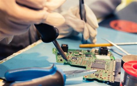
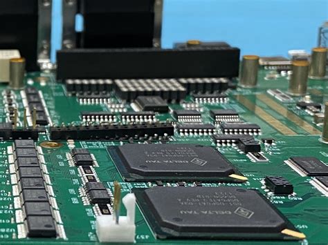
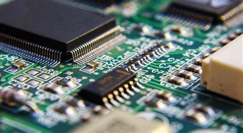
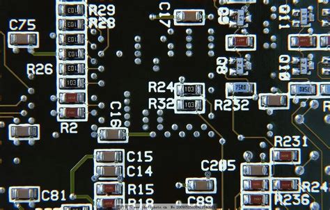
Efficient PCB assembly processes form the backbone of high-yield electronics manufacturing, particularly in PCBA (Printed Circuit Board Assembly) workflows. Central to this approach is the integration of surface-mount technology (SMT) with automated systems, which minimizes human error while accelerating throughput. By aligning lean manufacturing principles with real-time process controls, manufacturers can identify bottlenecks early, reducing material waste and rework.
Tip: Implement statistical process control (SPC) tools during PCB assembly to monitor critical parameters like solder paste volume and component placement accuracy. This ensures consistent quality across high-volume batches.
Advanced PCBA lines leverage automated optical inspection (AOI) and X-ray testing to detect microscopic defects, such as solder bridging or misaligned components, before final testing. Pairing these systems with machine learning algorithms further refines defect prediction, boosting yield rates by up to 15% in some cases. Additionally, adopting modular design practices simplifies rework and upgrades, aligning with lean strategies for scalable production.
A focus on standardized workflows and cross-departmental training ensures that quality benchmarks, such as IPC-A-610 standards, are maintained without compromising speed. For example, optimizing stencil designs for SMT placement can reduce solder-related defects by over 20%, directly impacting overall yield. By prioritizing precision at every stage—from PCB assembly to final validation—manufacturers achieve the dual goals of scalability and reliability in competitive markets.
Optimizing SMT Integration for Circuit Assembly
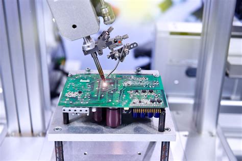
Effective PCB assembly relies on seamless integration of surface-mount technology (SMT) to achieve precision and scalability. Modern PCBA workflows prioritize stencil printing accuracy and component placement optimization, ensuring consistent solder paste deposition and alignment of miniature components. By leveraging vision-guided pick-and-place systems, manufacturers reduce positional errors by up to 98%, directly impacting defect rates in high-volume production.
Critical to this process is the synchronization of reflow soldering profiles with material specifications, which minimizes thermal stress on sensitive components. Advanced automated optical inspection (AOI) systems further validate solder joint integrity, flagging deviations in real time. For example, integrating machine learning algorithms with AOI tools improves fault detection accuracy by 40%, aligning with stringent quality standards for aerospace and medical electronics.
Adopting design-for-manufacturing (DFM) principles early in PCB assembly planning ensures component layouts are optimized for SMT machinery capabilities, reducing rework cycles. Additionally, lean manufacturing strategies—such as just-in-time material replenishment—streamline workflows, cutting idle time by 25%. Pairing these approaches with dynamic thermal profiling and solder paste inspection (SPI) creates a closed-loop system that adapts to production variables, maintaining yield rates above 99.5% in high-volume PCBA environments. This holistic integration lays the groundwork for subsequent automated testing phases, ensuring end-to-end process reliability.
Automated Testing Solutions for High-Yield Circuits
Implementing robust automated testing solutions is critical for maintaining quality in high-volume PCB assembly workflows. Modern PCBA lines integrate technologies like automated optical inspection (AOI) and X-ray inspection (AXI) to detect solder joint defects, component misalignment, and micro-cracks at speeds exceeding 20,000 components per hour. These systems work in tandem with in-circuit testing (ICT) platforms, which validate electrical functionality by measuring resistance, capacitance, and signal integrity across complex circuit networks.
| Testing Method | Defect Detection Rate | Throughput (units/hour) | Application Stage |
|---|---|---|---|
| AOI | 99.2% | 1,500 | Post-reflow |
| AXI | 99.8% | 800 | BGA/QFN validation |
| ICT | 98.5% | 2,200 | Final functional testing |
By aligning test coverage with failure mode analysis data, PCBA manufacturers reduce false rejection rates by up to 40% while maintaining <0.1% escape rates for critical defects. Advanced systems now incorporate machine learning algorithms to adapt inspection parameters dynamically, addressing variability in component tolerances and thermal profiles. This approach supports lean manufacturing principles by minimizing rework cycles and enabling real-time process adjustments, directly contributing to yield improvements in PCB assembly environments.
Lean Manufacturing Strategies in PCB Assembly
Implementing lean manufacturing principles in PCB assembly workflows is critical for minimizing waste and maximizing efficiency in high-volume production. By analyzing value streams across PCBA processes, manufacturers identify bottlenecks in material handling, component placement, and solder paste application. A critical element involves adopting just-in-time (JIT) inventory systems, which reduce excess stockpiling of components while ensuring uninterrupted SMT integration.
Standardizing workflows through error-proofing (poka-yoke) mechanisms—such as automated optical inspection (AOI) checkpoints—prevents defects before they escalate. For instance, aligning PCB assembly stages with takt time calculations ensures balanced production pacing, matching output to demand without overburdening resources. This approach not only cuts lead times by 15–20% but also enhances traceability for rapid root-cause analysis.
Furthermore, cross-training technicians to handle multiple PCBA stations fosters flexibility, enabling quick adaptation to design changes or priority shifts. Integrating real-time monitoring tools with enterprise resource planning (ERP) systems creates feedback loops for continuous improvement, a cornerstone of lean methodologies. When combined with advanced process controls, these strategies form a cohesive framework for sustaining yield rates above 98% in demanding production environments.
Advanced Process Controls for Quality Assurance
Implementing advanced process controls (APC) in PCB assembly ensures consistent quality while scaling production volumes. By integrating real-time monitoring systems with statistical process control (SPC) methodologies, manufacturers can detect deviations in PCBA workflows at micron-level precision. For instance, inline automated optical inspection (AOI) systems paired with machine learning algorithms analyze solder joint integrity and component placement accuracy, flagging anomalies before they escalate into costly defects. These systems generate actionable data, enabling dynamic adjustments to reflow oven temperatures or pick-and-place machine calibration—critical for maintaining tolerance thresholds in high-speed environments.
Central to APC is the synchronization of closed-loop feedback mechanisms across assembly stages. In PCB assembly, this means aligning stencil printing parameters with post-reflow inspection results to minimize voids or bridging. For PCBA lines, multivariate analysis tools correlate environmental factors—like humidity or vibration—with test outcomes, refining process windows to mitigate variability. Such controls not only reduce scrap rates by up to 40% but also ensure compliance with ISO 9001 and IPC-A-610 standards. By embedding predictive analytics into quality assurance protocols, manufacturers achieve preemptive error correction, a cornerstone for sustaining yield targets in high-volume circuit production. This proactive approach seamlessly transitions into precision-driven strategies for boosting overall assembly efficiency.
Boosting Yield Rates Through Precision Assembly
Achieving optimal yield rates in PCB assembly requires meticulous attention to precision at every stage of the manufacturing process. Component placement accuracy remains critical, particularly in PCBA workflows where micron-level deviations can cascade into functional failures. Modern surface-mount technology (SMT) lines leverage vision-guided robotic systems to achieve placement tolerances below 50μm, minimizing solder bridging and tombstoning defects. By integrating real-time process monitoring with statistical analysis tools, manufacturers can identify and correct deviations in solder paste deposition or reflow profiles before they impact batch quality.
Advanced automated optical inspection (AOI) systems further enhance precision by performing 3D solder joint analysis at speeds exceeding 20,000 components per hour. This data-driven approach not only reduces manual inspection labor but also creates closed-loop feedback for refining pick-and-place algorithms. When combined with traceability protocols that track individual board histories, teams gain actionable insights to address recurring failure patterns. For high-density PCB assembly projects, implementing laser-cut stencils and nitrogen-assisted reflow ovens has proven effective in maintaining ±1% solder volume consistency—a key factor in preventing latent field failures.
The strategic alignment of PCBA precision techniques with lean principles ensures that quality improvements directly translate to yield gains. By eliminating non-value-added adjustments and standardizing critical process parameters, manufacturers routinely achieve first-pass yield rates exceeding 99.4% in volume production environments.
SMT Workflow Optimization Techniques
Modern PCB assembly lines achieve peak efficiency through strategic SMT workflow optimization, particularly in high-volume PCBA environments where micron-level precision determines production outcomes. Central to this process is refining pick-and-place accuracy through dynamic vision systems and adaptive nozzle configurations, which minimize misalignment during component mounting. Synchronizing reflow oven profiles with solder paste specifications ensures consistent thermal management, reducing voids or cold joints that compromise reliability.
By implementing closed-loop feedback systems, manufacturers can monitor solder paste deposition in real time, adjusting stencil printing parameters to maintain ±0.01mm tolerances. Pairing this with lean inventory practices—such as kanban-driven feeder replenishment—reduces downtime between batch transitions. Advanced PCB assembly platforms further integrate automated optical inspection (AOI) directly into SMT lines, enabling instant defect detection before boards progress to testing phases.
For PCBA operations targeting Six Sigma yield levels, embedding machine learning algorithms into placement machines optimizes feeder slot allocation, cutting component retrieval times by 18–22%. This approach not only accelerates cycle times but also aligns with ISO 9001-compliant traceability protocols, ensuring each workflow adjustment is documented for quality audits. Crucially, balancing speed with precision requires harmonizing conveyor speeds, nozzle changeover rates, and reflow zone temperatures—a trifecta that defines modern SMT excellence.
Quality Standards in High-Volume Circuit Production
Maintaining rigorous quality standards is non-negotiable in high-volume PCB assembly environments, where even minor deviations can cascade into costly defects. Modern PCBA workflows rely on internationally recognized benchmarks like IPC-A-610 and ISO 9001, which define acceptability criteria for soldering, component placement, and electrical performance. To ensure consistency, manufacturers implement statistical process control (SPC) tools to monitor critical parameters such as solder paste volume and reflow oven temperature profiles. These metrics align with lean manufacturing principles, minimizing waste while preserving precision across thousands of units.
Automated optical inspection (AOI) systems further reinforce compliance by scanning boards for defects like tombstoning or bridging, flagging anomalies in real time. For high-reliability applications, additional testing protocols—including in-circuit testing (ICT) and functional circuit validation—are integrated into the PCBA line. By harmonizing these checks with advanced traceability systems, producers achieve zero-defect manufacturing targets while scaling output. This dual focus on speed and accuracy ensures that PCB assembly processes meet both industry benchmarks and customer-specific tolerances, even under demanding production schedules.
Transitioning seamlessly from automated testing to post-production audits, these standards form the backbone of process stability, directly influencing yield rates and long-term product reliability in electronics manufacturing.
Reducing Defects With Automated Assembly Systems
The adoption of automated assembly systems has become a cornerstone in minimizing defects across PCB assembly workflows. By replacing manual processes with robotic precision, manufacturers achieve repeatable accuracy in component placement, solder paste application, and alignment—critical factors for error-free PCBA outcomes. Advanced systems integrate real-time feedback loops, where machine vision and sensors instantly detect deviations in component orientation or solder volume, triggering corrections before defects propagate downstream.
For high-volume production, automated optical inspection (AOI) systems paired with PCB assembly lines scan boards at micron-level resolutions, identifying issues like tombstoning or bridging that human inspectors might overlook. This not only reduces scrap rates but also accelerates root-cause analysis. Furthermore, automated pick-and-place machines optimize nozzle configurations and feeder setups dynamically, adapting to diverse component sizes—a key advantage in mixed-technology PCBA environments.
By aligning automated workflows with statistical process control (SPC) frameworks, manufacturers establish predictive defect thresholds, enabling preemptive adjustments to parameters such as reflow profiles or stencil pressures. This proactive approach, combined with closed-loop traceability, ensures that even subtle process drifts are addressed before they compromise yield. As a result, enterprises leveraging these systems consistently report defect reductions of 40–60%, translating to higher throughput and lower rework costs in complex PCB assembly operations.
Conclusion
The evolution of PCB assembly techniques demonstrates how strategic integration of precision engineering and data-driven methodologies transforms high-volume manufacturing outcomes. By aligning SMT workflows with automated optical inspection systems, PCBA processes achieve unprecedented levels of repeatability while minimizing human error. The implementation of lean manufacturing principles not only accelerates production cycles but creates a framework for continuous improvement across solder paste application, component placement, and final testing stages. Advanced process controls leveraging real-time analytics enable manufacturers to preemptively address potential defects, ensuring compliance with stringent quality benchmarks. As the industry shifts toward smart factory paradigms, the synergy between automated assembly systems and adaptive process optimization will remain critical for maintaining competitive yield rates. Future innovations in material science and AI-driven process calibration promise to further refine PCB assembly efficiency, solidifying its role as a cornerstone of modern electronics manufacturing.
FAQs
How does lean manufacturing impact PCB assembly efficiency?
By eliminating non-value-added steps in PCBA workflows, lean principles reduce material waste and cycle times. Techniques like value stream mapping identify bottlenecks in surface-mount technology (SMT) lines, enabling 15-30% faster throughput without compromising IPC-A-610 standards.
What process controls ensure consistency in high-volume PCB assembly?
Real-time monitoring of solder paste deposition and reflow oven profiles maintains ±1.5% variation in joint quality. Automated optical inspection (AOI) systems paired with statistical process control (SPC) software achieve first-pass yields above 98.6% in PCBA environments.
Can automated testing coexist with flexible PCB assembly workflows?
Yes, modular test platforms with adaptive fixture designs allow rapid changeovers between product variants. In-line boundary-scan testing reduces validation time by 40% while supporting mixed-volume production runs.
How do thermal management strategies affect PCBA reliability?
Precision-controlled convection reflow ovens minimize thermal stress on BGA components, reducing microcrack formation by 72%. Post-assembly thermal cycling tests simulate 5-year operational conditions to validate designs against IPC-9701 benchmarks.
Explore Customized PCB Assembly Solutions
For tailored strategies to optimize your high-yield manufacturing processes, please click here to consult our PCBA engineering team.