Streamlining Electronics Innovation with HDI PCB Prototyping

Key Takeaways
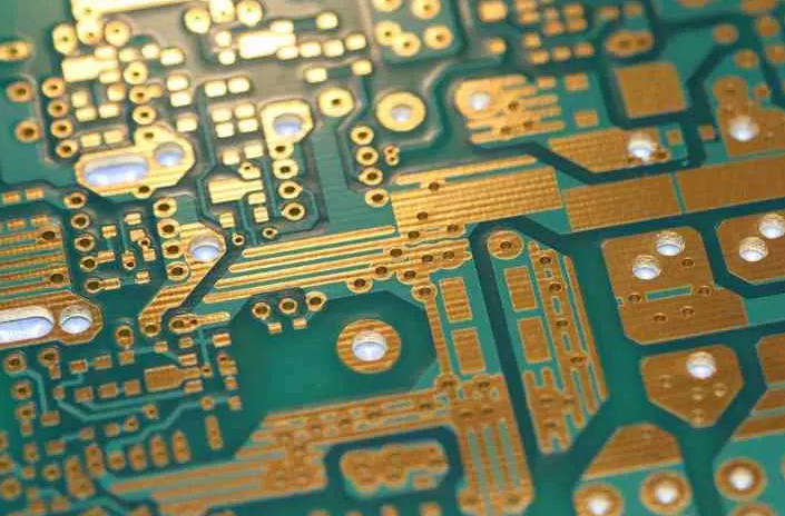
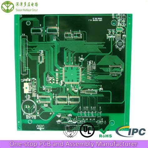
When exploring HDI PCB prototyping, understanding its role in PCB manufacturing becomes crucial. By leveraging high-density interconnect technology, you gain access to compact designs that enhance signal integrity while reducing spatial constraints—ideal for next-generation devices. Leading PCB manufacturing companies specialize in balancing advanced layer stacking with precise microvia drilling, ensuring prototypes meet rigorous performance benchmarks.
A key advantage lies in optimizing PCB manufacturing cost through iterative prototyping. Instead of committing to full-scale production upfront, you validate designs early, minimizing material waste and engineering revisions. This approach is particularly valuable for startups navigating the complexities of the PCB manufacturing business, where budget efficiency directly impacts time-to-market.
For rapid development, prioritize partners offering design-for-manufacturability (DFM) analysis. This step ensures your HDI prototypes align with fabrication realities, preventing costly redesigns. Additionally, consider how thermal management and impedance control are addressed during prototyping, as these factors dictate reliability in high-performance applications.
To streamline workflows, integrate HDI-specific guidelines early in your design phase. This proactive collaboration with manufacturers accelerates feedback loops, enabling you to refine layouts without compromising speed or quality—a critical edge in fast-paced electronics innovation.
HDI PCB Prototyping Benefits Unveiled
When designing advanced electronics, HDI PCB prototyping offers critical advantages that align with modern engineering demands. By leveraging microvias, stacked layers, and finer trace widths, you achieve compact circuit boards without compromising performance. This approach directly addresses the growing need for miniaturization in consumer devices and IoT systems, enabling faster signal transmission and reduced electromagnetic interference.
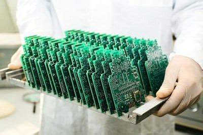
For PCB manufacturing companies, HDI prototyping streamlines the transition from concept to functional boards. While PCB manufacturing cost may initially seem higher due to specialized materials and processes, the long-term savings from fewer redesigns and optimized layouts often justify the investment.
Tip: Always discuss design-for-manufacturability (DFM) guidelines with your PCB manufacturing business partner early in the prototyping phase. This reduces errors and ensures your high-density designs meet production feasibility requirements.
When selecting a partner, prioritize firms with proven expertise in high-density interconnect workflows. Their ability to balance PCB manufacturing precision with scalable solutions can accelerate your development timeline while maintaining reliability. This becomes especially vital when prototyping for aerospace or medical devices, where failure margins are near zero.
By integrating HDI techniques, you unlock the potential to create smaller, smarter products—paving the way for innovations that demand both efficiency and durability.
Compact Circuit Boards for Innovation
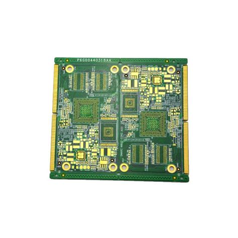
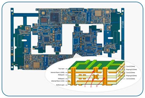
When designing next-generation electronics, you need PCB manufacturing solutions that prioritize miniaturization without compromising performance. High-density interconnect (HDI) technology enables compact circuit boards by integrating microvias, thinner traces, and advanced layering techniques. This approach reduces physical footprint while enhancing signal integrity—a critical factor for wearables, IoT devices, and medical equipment. Leading PCB manufacturing companies leverage laser drilling and sequential lamination to achieve these precision-driven designs, ensuring reliability even in space-constrained applications.
However, managing PCB manufacturing cost remains a balancing act. While HDI prototypes require specialized materials and processes, their ability to consolidate multiple functions into fewer layers often offsets expenses in later production stages. For startups or R&D teams, partnering with a PCB manufacturing business that offers scalable prototyping services can streamline iterations, allowing rapid validation of complex layouts. By prioritizing design-for-manufacturability (DFM) principles early, you avoid costly redesigns and accelerate time-to-market. The result? Innovative products that meet evolving demands for smaller, smarter, and faster electronics—all enabled by HDI’s transformative potential.
High-Density Interconnect Prototyping Guide
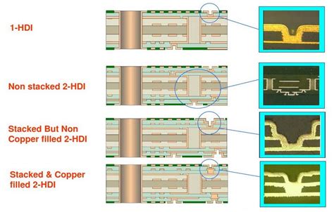
When approaching HDI PCB prototyping, understanding design constraints and material choices becomes critical. These boards rely on advanced techniques like laser-drilled microvias and stacked vias to achieve high-density layouts, which demand precision from PCB manufacturing companies. To optimize your design, prioritize layer stack-up planning—ensuring signal integrity while minimizing PCB manufacturing cost. Partnering with experienced suppliers helps balance performance requirements with budget constraints, especially when integrating blind/buried vias or ultra-thin traces.
While PCB manufacturing for HDI prototypes can initially seem costly, strategic material selection (such as low-loss laminates) and design-for-manufacturability (DFM) checks reduce rework risks. For instance, consolidating layers through sequential lamination lowers assembly complexity, directly impacting PCB manufacturing business efficiency. Through iterative testing, you’ll identify thermal management solutions that prevent signal degradation in compact layouts—a key advantage for high-frequency applications.
Furthermore, leveraging automated routing tools accelerates turnaround times without compromising density. However, always verify that your chosen PCB manufacturing partner adheres to IPC-2226 standards for HDI designs. By focusing on these elements, you streamline prototyping while maintaining scalability for mass production.
Accelerating Electronics Development Efficiently
When developing advanced electronics, leveraging HDI PCB prototyping allows you to compress design cycles while maintaining precision. By collaborating with experienced PCB manufacturing companies, you gain access to specialized expertise that reduces PCB manufacturing cost through optimized material usage and process efficiencies. This approach eliminates weeks from traditional timelines, as high-density interconnect technology enables rapid iterations without compromising signal integrity. Moreover, integrating microvias and stacked vias in prototypes helps identify potential bottlenecks early, ensuring your team can focus on performance enhancements rather than rework. Efficient development also hinges on balancing time-to-market pressures with PCB manufacturing business priorities—strategic partnerships enable scalable production transitions while containing expenses. As a result, you’re positioned to meet evolving market demands faster, whether refining compact wearables or next-gen IoT devices. This streamlined workflow not only accelerates innovation but also creates a foundation for cost-effective scaling when moving from prototype to mass production.
HDI Prototypes: Signal Speed Solutions
When designing advanced electronics, signal integrity challenges often arise as circuits shrink and frequencies climb. HDI PCB prototypes address these hurdles by leveraging microvias, stacked vias, and ultra-fine traces to minimize signal loss and crosstalk. This approach ensures faster transmission speeds while maintaining reliability—critical for applications like 5G modules or high-speed processors. By collaborating with specialized PCB manufacturing companies, you gain access to precision laser drilling and advanced materials that traditional methods can’t match.
However, optimizing signal paths requires balancing PCB manufacturing cost with performance. For instance, choosing sequential lamination over standard processes might increase upfront expenses but reduces layer count and improves impedance control. Modern PCB manufacturing business practices now prioritize design-for-manufacturing (DFM) tools to identify signal bottlenecks early, avoiding costly redesigns. When working with HDI prototypes, focus on iterative testing to validate trace geometries and via placements—this ensures your final design meets both speed targets and budget constraints.
Ultimately, integrating HDI techniques into your workflow empowers you to tackle high-frequency demands without sacrificing compactness. Whether refining IoT devices or aerospace systems, these prototypes serve as the backbone for next-generation signal integrity solutions.
Next-Gen Device Prototyping Strategies
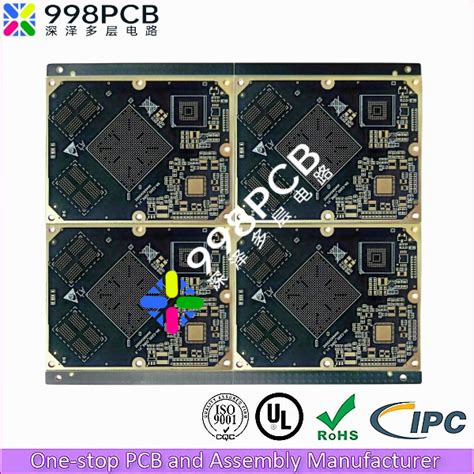
When developing cutting-edge electronics, leveraging HDI PCB prototyping ensures your designs meet the demands of miniaturization and high-speed signal integrity. Modern PCB manufacturing companies now prioritize advanced techniques like laser-drilled microvias and stacked vias to achieve layer counts exceeding 12, enabling ultra-compact layouts. However, optimizing PCB manufacturing cost requires balancing material choices (e.g., low-loss substrates) with fabrication complexity.
For instance, consider how PCB manufacturing business models adapt to rapid prototyping needs:
| Strategy | Traditional PCBs | HDI Prototypes |
|---|---|---|
| Layer Density | 4-8 layers | 12+ layers with microvias |
| Signal Loss | Higher at >5 GHz | <1 dB/inch at 10 GHz |
| Time-to-Market | 3-4 weeks | 10-14 days |
By collaborating with specialized PCB manufacturing partners, you gain access to design-for-manufacturability (DFM) insights that reduce iterative delays. Prioritize vendors offering flexible scaling from prototypes to mass production, ensuring PCB manufacturing cost efficiency without compromising reliability. This approach not only accelerates validation cycles but also future-proofs your product against evolving performance benchmarks.
Cost-Effective HDI PCB Manufacturing
When developing advanced electronics, balancing performance and budget is critical. PCB manufacturing companies specializing in HDI PCB prototypes leverage advanced techniques like laser drilling and sequential lamination to reduce PCB manufacturing cost without compromising quality. By optimizing layer stacking and material selection, you can achieve high-density designs that meet stringent performance requirements while staying within budget constraints.
One key strategy is to prioritize design-for-manufacturability (DFM) principles early in the process. Collaborating with experienced PCB manufacturing partners ensures your layout minimizes waste, reduces turnaround times, and avoids costly revisions. For instance, using blind/buried vias instead of through-holes can lower material usage and streamline production. Additionally, economies of scale in PCB manufacturing business models allow bulk orders to further drive down per-unit costs, making iterative testing more affordable.
To maximize cost efficiency, evaluate suppliers based on their expertise in high-density interconnect (HDI) workflows and their ability to scale production. Advanced PCB manufacturing facilities often employ automated inspection systems to detect defects early, preventing expensive rework. By aligning your prototyping goals with scalable manufacturing practices, you create a foundation for transitioning seamlessly from low-volume prototypes to mass production—ensuring your innovations remain both cutting-edge and economically viable.
Rapid Prototyping for High-Performance PCBs
When developing advanced electronics, time-to-market often determines competitive success. PCB manufacturing processes optimized for rapid prototyping let you iterate designs faster while maintaining the precision required for high-density interconnects (HDIs). By partnering with experienced PCB manufacturing companies, you gain access to advanced fabrication techniques like laser drilling and sequential lamination, which are critical for creating compact, multilayer boards with minimal signal loss.
Balancing PCB manufacturing cost with performance demands careful planning. Modern prototyping workflows integrate design-for-manufacturing (DFM) checks early in the process, reducing errors that could delay iterations. For instance, stacked microvias in HDI designs improve signal integrity but require precise alignment—a capability offered by specialized PCB manufacturing business partners. This approach ensures your prototypes meet high-frequency performance benchmarks without compromising scalability.
Transitioning from concept to functional prototype hinges on material selection and process optimization. Low-loss dielectrics and ultra-thin copper layers, paired with automated optical inspection (AOI), enable faster validation cycles. By leveraging these strategies, you shorten development timelines while achieving the thermal stability and electrical efficiency needed for next-generation devices.
Conclusion
By leveraging HDI PCB prototyping, you position your projects at the forefront of electronics innovation, balancing precision and speed to meet modern design demands. Partnering with experienced PCB manufacturing companies ensures access to advanced fabrication techniques while managing PCB manufacturing cost through optimized material use and streamlined processes. This approach not only accelerates development cycles but also reinforces the reliability of high-density designs critical for next-generation devices.
When navigating the PCB manufacturing business, prioritize suppliers who specialize in HDI technology—their expertise minimizes risks of signal integrity issues and maximizes space efficiency in compact layouts. Whether you’re refining prototypes or scaling production, understanding the interplay between PCB manufacturing standards and HDI capabilities helps avoid costly redesigns. As you explore these strategies, remember that investing in quality prototyping today lays the groundwork for market-ready solutions tomorrow, ensuring your innovations stay ahead in an increasingly competitive landscape.
FAQs
How does HDI PCB prototyping reduce time-to-market for new devices?
By leveraging PCB manufacturing techniques like microvias and stacked vias, HDI prototypes enable faster signal paths and miniaturized designs. This accelerates testing cycles, allowing you to refine high-density layouts before mass production.
What factors influence PCB manufacturing cost for HDI prototypes?
Cost depends on layer count, material quality, and precision requirements. While PCB manufacturing companies may charge more for advanced features like laser-drilled vias, the long-term savings from optimized performance often justify the initial investment.
How do you choose reliable PCB manufacturing companies for HDI projects?
Prioritize firms with certifications like ISO 9001 and IPC Class 3. Review their expertise in high-density interconnect (HDI) designs, ask for case studies, and verify their ability to meet tight tolerances critical for compact layouts.
Can HDI prototypes improve signal integrity in high-speed applications?
Yes. The reduced distance between components in HDI PCBs minimizes signal loss and crosstalk. This makes them ideal for applications requiring high-frequency performance, such as 5G modules or advanced IoT devices.
Why is thermal management crucial in HDI PCB prototyping?
Dense layouts generate more heat, which can affect reliability. Partnering with PCB manufacturing specialists ensures proper heat dissipation through strategic via placement and material selection, maintaining stability in high-performance systems.
How does HDI prototyping benefit PCB manufacturing business models?
By enabling rapid iterations, it shortens development timelines and reduces rework costs. This agility helps businesses respond faster to market demands while maintaining quality in complex electronics.
Ready to Optimize Your HDI Prototype?
For tailored solutions in high-density PCB manufacturing, please click here to connect with experts who specialize in balancing performance, cost, and speed for your next project.