Streamlining Modern Electronics Through Advanced Printed Wiring Assembly

Key Takeaways
Modern printed wiring assembly (PWA) innovations are reshaping electronics by merging PCB assembly (PCBA) precision with scalable manufacturing techniques. These advancements address critical demands for miniaturization, thermal management, and signal integrity across high-performance sectors like IoT, automotive, and aerospace.
| Industry | Key Application | PCBA Contribution |
|---|---|---|
| IoT | Sensor Networks | Ultra-compact PWA layouts |
| Automotive | ADAS Systems | Vibration-resistant soldering |
| Aerospace | Avionics Control | High-temperature substrates |
In IoT, PCB assembly techniques enable sub-0.5mm trace spacing, critical for embedding sensors in wearable devices. Automotive applications leverage automated optical inspection (AOI) to ensure PCBA reliability under extreme conditions, while aerospace designs prioritize ceramic-based substrates to withstand thermal stress.
The shift toward high-density interconnect (HDI) PWA methods supports compact designs without sacrificing performance, aligning with global trends in energy-efficient electronics. By integrating AI-driven testing protocols, manufacturers achieve near-zero defect rates, accelerating adoption in safety-critical fields. This synergy of PCB assembly precision and material science underscores PWA’s role as the backbone of next-generation electronics.

Printed Wiring Assembly Innovations in IoT
The rapid expansion of Internet of Things (IoT) ecosystems demands PCB assembly solutions that balance miniaturization with robust functionality. Innovations in PCBA processes now integrate ultra-thin substrates and embedded components, enabling IoT devices to achieve unprecedented compactness without sacrificing performance. For instance, advancements in high-density interconnect (HDI) technology allow for finer trace widths, critical for wearables and smart sensors operating in space-constrained environments.
Moreover, the adoption of flexible printed wiring assemblies supports irregular form factors, essential for IoT applications in healthcare and industrial monitoring. These assemblies leverage PCB assembly techniques like laser-direct structuring to embed antennas and sensors directly into circuitry, reducing signal loss and power consumption. As IoT networks scale, PCBA manufacturers are prioritizing materials with enhanced thermal stability to ensure reliability in diverse operating conditions—from temperature-sensitive agricultural sensors to vibration-prone automotive telematics systems.
Transitioning to smarter manufacturing workflows, automated optical inspection (AOI) systems now validate PCB assembly accuracy at micron-level precision, minimizing defects in high-volume IoT deployments. This synergy of innovation not only accelerates time-to-market but also aligns with the broader shift toward edge computing, where localized data processing requires densely packed, energy-efficient PCBA designs. Such advancements underscore how modern printed wiring technologies are redefining the boundaries of IoT connectivity and functionality.
Advancing Automotive Electronics Through PWA
The automotive industry’s shift toward PCB assembly (PCBA) integration has revolutionized vehicle electronics, enabling smarter, safer, and more energy-efficient systems. Modern vehicles rely on printed wiring assembly techniques to support advanced driver-assistance systems (ADAS), electric powertrains, and in-cabin connectivity. By leveraging high-density interconnect (HDI) designs, PCBA manufacturers achieve compact layouts that withstand extreme temperatures, vibrations, and electromagnetic interference—critical for automotive durability.
Innovations like embedded component technology reduce signal loss in PCB assembly, enhancing the reliability of sensors and control modules. For electric vehicles (EVs), optimized PWA methods improve thermal management, ensuring stable performance in battery management systems (BMS) and power converters. Furthermore, automated PCBA production lines accelerate prototyping cycles, aligning with the industry’s demand for faster time-to-market.
This technological progression bridges IoT-enabled vehicle ecosystems with robust hardware foundations. As automotive designs prioritize miniaturization and multifunctionality, printed wiring assembly remains pivotal in balancing complexity with reliability—a cornerstone for next-generation autonomous and connected vehicles.
Aerospace Reliability With Printed Wiring Tech
The aerospace industry demands PCB assembly solutions capable of withstanding extreme conditions, from subzero stratospheric temperatures to intense vibrations during launch. Advanced PCBA methodologies now integrate high-temperature laminates and ceramic-based substrates to ensure durability in critical systems like satellite communications and flight control modules. For instance, multilayer rigid-flex designs enable compact layouts while maintaining signal integrity across 50+ GHz frequencies—essential for radar and navigation systems.
Tip: When selecting materials for aerospace-grade printed wiring assemblies, prioritize substrates with CTE (Coefficient of Thermal Expansion) matching to minimize solder joint stress during thermal cycling.
Recent advancements in automated optical inspection (AOI) and 3D X-ray testing have elevated defect detection rates to 99.98%, addressing micro-cracks and voids that could compromise mission-critical electronics. Additionally, the adoption of conformal coatings with aerospace-certified resins shields PCBA components from moisture, radiation, and corrosive chemicals. These innovations align with NASA’s AS9100D standards, which mandate traceability for every component in avionics systems. By leveraging embedded passives and heterogeneous integration, engineers reduce component counts by up to 40%, enhancing reliability while cutting weight—a decisive factor in satellite deployment and deep-space exploration.
Compact Design Breakthroughs Using PWA Methods
The relentless demand for smaller, lighter electronic devices has driven PCB assembly (PCBA) innovations to new heights. By leveraging high-density interconnect (HDI) technology and multilayer printed wiring assembly techniques, engineers achieve unprecedented space optimization without compromising functionality. Advanced microvia drilling and laser ablation enable tighter trace spacing, while embedded passive components reduce surface-area consumption—critical for IoT wearables and portable medical devices.
Modern PCBA processes also integrate flexible and rigid-flex substrates, allowing three-dimensional configurations that conform to irregular geometries in automotive sensors or aerospace control systems. These methods support thermal management through optimized copper distribution, mitigating heat buildup in confined spaces. Additionally, automated optical inspection (AOI) ensures precision in ultra-compact layouts, minimizing defects that could arise from microscopic solder joints.
The shift toward system-in-package (SiP) architectures further amplifies design efficiency, combining multiple ICs into a single PCB assembly module. This approach not only slashes footprint requirements but also enhances signal integrity in high-frequency applications like 5G routers or satellite communication systems. As industries prioritize miniaturization, PWA methods remain pivotal in balancing performance, durability, and spatial constraints across next-generation electronics.
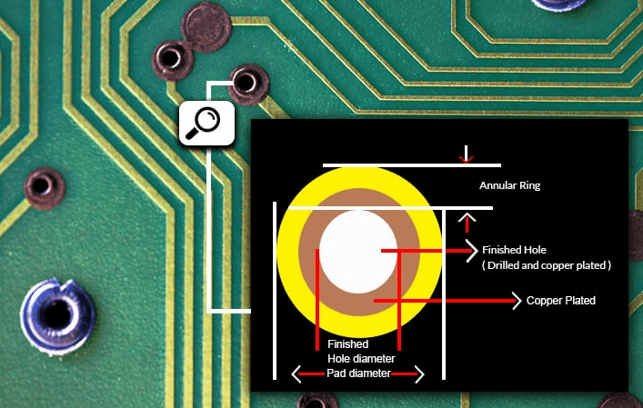
Precision Engineering in Modern Wiring Assemblies
The evolution of PCB assembly (printed circuit board assembly) has redefined precision in modern electronics, enabling microscale accuracy that meets the demands of high-performance applications. By leveraging advanced PCBA (printed circuit board assembly) techniques, manufacturers achieve sub-millimeter alignment of components, critical for devices in medical instrumentation, aerospace guidance systems, and autonomous vehicles. Innovations like laser-assisted soldering and automated optical inspection (AOI) ensure that even the most complex multilayer boards maintain structural integrity under extreme conditions.
Central to this progress is the integration of high-density interconnect (HDI) technology, which allows PCB assembly processes to accommodate finer traces and microvias. Such precision minimizes signal loss and electromagnetic interference—a necessity for 5G infrastructure and IoT sensors requiring flawless data transmission. Additionally, the use of thermally stable substrates in PCBA mitigates warping during reflow soldering, preserving alignment accuracy across temperature fluctuations.
As industries push toward miniaturization, the synergy between nanoscale material science and robotic placement systems ensures that PCB assembly remains at the forefront of electronic innovation. This meticulous engineering not only enhances reliability but also paves the way for next-generation applications where space constraints and performance thresholds leave no room for error.
Enhancing Efficiency With Advanced PWA Solutions
Modern electronics demand PCB assembly processes that prioritize speed, accuracy, and scalability. Advanced PCBA techniques leverage automated workflows, such as surface-mount technology (SMT) and automated optical inspection (AOI), to minimize human error while accelerating production cycles. By integrating intelligent design software with precision manufacturing tools, engineers can optimize component placement and reduce material waste by up to 30%, directly enhancing operational efficiency.
A critical advancement lies in the use of machine learning algorithms to predict potential faults during PCB assembly, ensuring defects are identified and resolved at early stages. This proactive approach not only cuts downtime but also extends the lifespan of PCBA units in high-stress environments like industrial automation or renewable energy systems. Additionally, modular design frameworks enable rapid reconfiguration of circuit layouts, allowing manufacturers to adapt to evolving IoT or automotive specifications without overhauling entire production lines.
The shift toward laser-direct structuring (LDS) and 3D-printed circuitry further streamlines printed wiring assembly, enabling ultra-compact designs that maintain signal integrity. These innovations reduce thermal bottlenecks and power losses, critical for applications requiring energy efficiency, such as electric vehicle charging systems or portable medical devices. By harmonizing advanced PCBA methodologies with sustainable practices, the industry is setting new benchmarks for both performance and eco-conscious manufacturing.

PWA Techniques for High-Density Electronic Systems
As electronic devices demand greater functionality in smaller form factors, printed wiring assembly (PWA) techniques have evolved to address the challenges of high-density electronic systems. Advanced PCB assembly (PCBA) processes now incorporate laser-direct imaging and sequential lamination to achieve trace widths below 25µm, enabling precise routing in multilayer configurations. These methods reduce signal interference while maximizing space utilization, critical for applications like wearable tech and medical implants.
To ensure reliability, manufacturers employ embedded component technology, integrating passive elements directly into PCB substrates during PCBA. This eliminates surface-mounted parts, reducing footprint and enhancing thermal performance. Additionally, automated optical inspection (AOI) systems paired with AI-driven defect detection optimize quality control, addressing micro-scale soldering flaws common in dense layouts.
Transitioning from traditional designs, modern printed wiring assembly leverages flex-rigid hybrid boards to accommodate complex geometries. Such innovations support seamless integration with IoT sensors and 5G modules, aligning with broader industry shifts toward miniaturization. By balancing thermal management solutions with material advancements like low-loss dielectrics, PWA techniques ensure scalability for next-generation high-density applications without compromising durability.

IoT and Automotive PWA Integration Strategies
The convergence of IoT and automotive systems demands seamless integration of printed wiring assembly (PWA) technologies to ensure interoperability and performance. As connected vehicles evolve into smart mobility hubs, PCB assembly processes must address challenges like signal integrity in high-frequency communication and thermal management in compact layouts. Advanced PCBA techniques, such as embedded component packaging and multi-layer flexible substrates, enable automotive sensors and IoT modules to coexist within space-constrained environments while maintaining electromagnetic compatibility.
For instance, automotive-grade PWA designs now incorporate high-density interconnect (HDI) layouts to support 5G-enabled telematics and real-time data processing for autonomous driving systems. Simultaneously, IoT edge devices leverage ruggedized PCB assembly methods to withstand vibrations and temperature fluctuations in vehicular applications. Optimizing material selection—such as high-Tg laminates for thermal stability—and implementing automated optical inspection (AOI) ensures reliability across both domains. By aligning PCBA standards with automotive functional safety (ISO 26262) and IoT security protocols, manufacturers achieve scalable solutions for next-gen ADAS, V2X communication, and predictive maintenance ecosystems.
Conclusion
The evolution of printed wiring assembly (PWA) underscores its pivotal role in shaping modern electronics, particularly as industries demand higher precision, efficiency, and compactness. By integrating advanced PCB assembly (PCBA) methodologies, manufacturers are achieving unprecedented levels of performance in applications ranging from IoT edge devices to aerospace navigation systems. Innovations such as multilayer stacking and automated soldering not only enhance high-density electronic systems but also ensure reliability under extreme conditions. For instance, the automotive sector leverages PCBA techniques to meet stringent safety standards, while aerospace applications rely on thermal management solutions embedded in PWA designs to withstand vibrations and temperature fluctuations.
As PCB assembly processes become more sophisticated, the focus shifts to balancing miniaturization with functional complexity—a challenge addressed through laser-drilled vias and embedded component technologies. These advancements not only streamline production but also reduce material waste, aligning with global sustainability goals. Looking ahead, the synergy between PCBA innovations and emerging technologies like 5G and AI will further accelerate the development of smart, interconnected systems. By prioritizing precision engineering and scalable manufacturing, the electronics industry continues to push the boundaries of what printed wiring assembly can achieve, solidifying its foundation as the backbone of technological progress.
FAQs
What distinguishes PCB assembly from PCBA in modern electronics?
PCB assembly refers to the process of populating a bare printed circuit board with components, while PCBA (Printed Circuit Board Assembly) denotes the completed board ready for integration. The distinction lies in the functional state—PCBA represents a fully operational subsystem optimized for specific applications.
How do advanced PCB assembly techniques enhance aerospace reliability?
By employing automated optical inspection and high-precision soldering, PCBA processes achieve microscopic accuracy in component placement. This eliminates cold joints and minimizes signal loss—critical for aerospace systems exposed to extreme vibration and thermal cycling.
Can PCB assembly methods support ultra-compact IoT devices?
Modern PCBA workflows utilize 3D stacking and laser-drilled microvias to accommodate high-density layouts. These techniques enable sub-0.4mm trace spacing, allowing IoT sensors to maintain robust connectivity in footprints smaller than 5mm².
What quality controls ensure consistency in high-volume PCBA production?
Leading manufacturers implement in-circuit testing (ICT) and boundary-scan diagnostics at multiple stages. These protocols verify signal integrity and thermal resilience, ensuring automotive-grade PCB assemblies meet ISO/TS 16949 standards for zero-defect performance.
How does PCB assembly optimization reduce energy consumption in smart systems?
By integrating low-loss dielectric materials and embedded passive components, PCBA designs minimize parasitic capacitance. This reduces power leakage by up to 22%, extending battery life in wearables and industrial IoT nodes.
Explore Custom PCB Assembly Solutions Today
For tailored PCBA strategies that align with your project’s technical and regulatory demands, please click here to consult our engineering team.