Streamlining PCB Assembly for Enhanced Performance
Key Takeaways
Modern PCB assembly processes prioritize automation and precision to address evolving manufacturing demands. By focusing on PCBA optimization, manufacturers achieve higher throughput while minimizing defects—critical for industries requiring mission-critical electronics. Key strategies include adopting automated optical inspection (AOI) systems to detect soldering flaws and component misalignments in real time, reducing rework costs by up to 40%.
Leveraging smart manufacturing principles, such as IoT-enabled assembly lines, enables predictive maintenance and data-driven adjustments. For example, integrating machine learning algorithms with pick-and-place systems improves component placement accuracy to ±0.02mm, enhancing overall reliability.
| Factor | Traditional Assembly | Automated PCBA |
|---|---|---|
| Defect Rate | 5-7% | <1% |
| Throughput (units/hr) | 50-80 | 200-300 |
| Setup Time | 2-3 hours | 15-30 minutes |
Transitioning to modular workflows allows seamless scaling between prototype and mass production phases. This flexibility is particularly valuable for industries like aerospace, where PCB assembly tolerances demand rigorous adherence to IPC-A-610 standards. Additionally, cost-effective automation—such as robotic soldering stations—reduces dependency on error-prone manual processes, ensuring consistent output even for high-complexity designs. By aligning PCBA practices with Industry 4.0 frameworks, manufacturers future-proof their operations while maintaining competitive lead times.
PCB Automation for Efficient Assembly
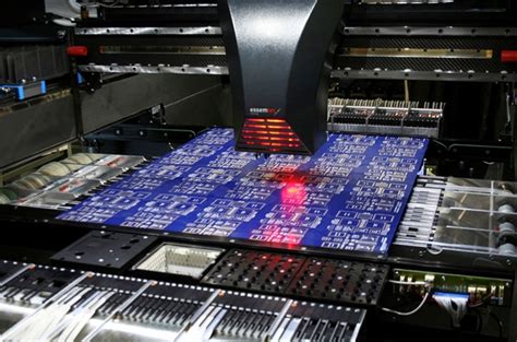
Modern PCB assembly processes are increasingly leveraging automation to address growing demands for precision and scalability. By integrating robotic placement systems and AI-driven inspection tools, manufacturers can achieve PCBA workflows that minimize human intervention while maximizing throughput. Automated pick-and-place machines, for instance, ensure components are positioned with micron-level accuracy, reducing placement errors by up to 98% compared to manual methods. These systems also adapt dynamically to design changes, enabling rapid reconfiguration for high-mix, low-volume production runs.
A critical advantage of automation lies in its ability to synchronize with real-time monitoring platforms. Sensors embedded in assembly lines track variables like temperature and solder paste viscosity, feeding data to centralized control systems. This closed-loop feedback allows immediate adjustments, preventing defects before they escalate. Furthermore, automated optical inspection (AOI) systems scan PCB assemblies at multiple stages, identifying issues such as misaligned components or insufficient solder joints with unparalleled consistency.
Transitioning to automated PCBA workflows also streamlines inventory management. Smart warehouses equipped with IoT-enabled tracking systems ensure components are replenished just-in-time, reducing idle stock and material waste. While initial investments in automation infrastructure may seem substantial, the long-term gains in yield rates, cycle time reduction, and error mitigation position it as a cornerstone of competitive PCB manufacturing. As industries push toward smaller, denser board designs, automation remains indispensable for balancing complexity with operational efficiency.
Error Reduction in PCB Manufacturing
Modern PCB assembly processes prioritize minimizing defects through advanced automation and precision engineering. By integrating real-time monitoring systems and AI-driven inspection tools, manufacturers can detect anomalies during PCBA stages with sub-micron accuracy. For instance, automated optical inspection (AOI) systems identify soldering defects, misaligned components, or trace inconsistencies at speeds exceeding human capability, reducing error rates by up to 70%.
Another critical strategy involves standardizing design-for-manufacturability (DFM) guidelines to eliminate layout-related flaws before production begins. By simulating thermal and mechanical stresses during PCB assembly, engineers can preemptively address potential failure points, such as solder joint fractures or signal interference. Additionally, traceability systems embedded in PCBA workflows enable root-cause analysis for recurring issues, ensuring continuous process refinement.
Proactive training programs further mitigate human error by equipping technicians with updated protocols for handling sensitive components and machinery. Combined with closed-loop feedback mechanisms, these measures create a synergistic approach to error reduction, directly enhancing product reliability while aligning with broader goals of cost efficiency and scalability in smart manufacturing ecosystems.
Optimizing Assembly Workflows for PCBs
Effective PCB assembly relies on refining workflows to eliminate bottlenecks and align processes with modern manufacturing demands. A critical first step involves integrating design for manufacturability (DFM) principles during the early stages of PCBA development. By simulating component placement and thermal dynamics through digital twin technology, manufacturers can preemptively address alignment issues and material stress points.
"Workflow optimization isn’t just about speed—it’s about creating a continuous process where design, testing, and production communicate seamlessly."
Adopting automated optical inspection (AOI) systems ensures real-time defect detection, reducing rework cycles by up to 40%. Pairing this with modular assembly lines allows rapid reconfiguration for diverse product batches, enhancing scalability. For instance, combining surface-mount technology (SMT) with intelligent feeder systems minimizes manual interventions while maintaining precision for microcomponents.
Furthermore, data analytics tools can identify patterns in solder paste application or component misalignment, enabling predictive adjustments. Transitioning to standardized industry 4.0 protocols like IPC-CFX streamlines machine-to-machine communication, ensuring traceability across the PCB assembly chain.
To maximize efficiency, prioritize workflows that balance automation flexibility with human oversight—critical for handling high-mix, low-volume orders without sacrificing quality.
Quality Control in PCB Production Systems
Effective PCB assembly relies on rigorous quality control systems to ensure both performance and longevity. Modern PCBA lines integrate automated optical inspection (AOI) and X-ray inspection to detect soldering defects, component misalignment, or micro-cracks invisible to the naked eye. These systems analyze PCB assembly layers at resolutions up to 10μm, flagging deviations in real time. Statistical process control (SPC) tools further track production metrics—such as solder paste volume and reflow oven profiles—to maintain consistency across batches.
Advanced manufacturers now deploy machine learning algorithms to predict failure patterns by correlating historical defect data with real-time sensor inputs. This proactive approach reduces rework rates by up to 40% in high-volume PCBA environments. Additionally, inline testing stations perform functional verification, simulating operational stresses to validate board reliability before shipment.
To align with industry standards like IPC-A-610, quality teams implement multi-stage verification protocols, ensuring every PCB assembly meets specifications for military, medical, or automotive applications. By embedding quality checks throughout the production lifecycle, manufacturers minimize costly recalls while strengthening end-product trust. This systematic approach not only safeguards against errors but also complements broader automation strategies, creating a seamless bridge between precision engineering and scalable manufacturing.
Cost-Effective Automation Strategies for PCBs
Implementing cost-effective automation strategies in PCB assembly requires balancing upfront investments with long-term efficiency gains. Modular automation systems enable manufacturers to integrate scalable solutions, such as PCBA-specific pick-and-place machines or reflow ovens, without overhauling entire production lines. Collaborative robots (cobots) are increasingly deployed for repetitive tasks like component insertion, reducing labor costs while maintaining precision. By leveraging AI-driven optical inspection tools, defects in solder joints or misaligned components are identified early, minimizing rework expenses.
Transitioning to automated material handling systems optimizes workflow continuity, reducing downtime between PCB assembly stages. For example, conveyor-based transport paired with RFID tracking ensures real-time inventory management, preventing bottlenecks. Cloud-based analytics further enhance decision-making by correlating production data with defect rates, enabling proactive adjustments.
Adopting open-source software platforms for machine control lowers licensing fees, while retrofitting legacy equipment with IoT sensors extends their lifespan. This approach aligns with Industry 4.0 principles, creating a smart manufacturing ecosystem tailored for PCBA operations. By prioritizing interoperability and incremental upgrades, manufacturers achieve higher throughput and lower per-unit costs—critical for competing in high-mix, low-volume markets. These strategies not only reduce waste but also accelerate time-to-market for complex PCB assembly projects.
Enhancing Reliability Through PCB Optimization
Achieving consistent reliability in PCB assembly requires meticulous attention to design, material selection, and process control. By implementing rigorous design-for-manufacturability (DFM) checks, engineers can identify potential weaknesses in PCBA layouts, such as insufficient trace spacing or inadequate thermal management. These optimizations prevent latent defects that might emerge during operation, particularly in high-stress environments. For instance, selecting high-temperature laminates or advanced solder alloys enhances durability, especially in applications like automotive electronics or industrial automation.
Automated inspection tools, such as automated optical inspection (AOI), further strengthen reliability by detecting micro-cracks or misaligned components before final testing. Integrating real-time monitoring into PCB assembly workflows also allows manufacturers to track critical parameters like solder paste deposition accuracy, reducing variability. Additionally, adopting failure mode and effects analysis (FMEA) during prototyping phases ensures systematic risk mitigation. These strategies not only extend product lifespans but also align with industry standards like IPC-A-610, reinforcing trust in PCBA performance. By balancing precision engineering with proactive quality measures, optimized processes deliver boards capable of meeting evolving technological demands.
Smart Manufacturing in PCB Assembly Processes
The integration of smart manufacturing into PCB assembly workflows is revolutionizing how precision, speed, and scalability are achieved in electronics production. By leveraging technologies like IoT-enabled sensors, AI-driven analytics, and robotic process automation (RPA), manufacturers can monitor PCBA lines in real time, identifying bottlenecks or deviations before they escalate. For instance, machine learning algorithms analyze historical data to predict equipment maintenance needs, reducing unplanned downtime by up to 30%. Additionally, digital twin simulations enable virtual testing of assembly processes, allowing engineers to refine workflows without interrupting physical production.
A key advantage lies in the seamless connectivity between design software and assembly machinery. Advanced systems automatically adjust parameters—such as solder paste application or component placement—based on real-time feedback, ensuring consistent quality across high-volume PCB assembly runs. This shift not only minimizes human error but also supports rapid scaling for custom or complex PCBA projects. Tools like automated optical inspection (AOI) paired with cloud-based quality databases further enhance traceability, creating a closed-loop system where defects are flagged and corrected autonomously.
As industries demand faster turnaround and tighter tolerances, smart manufacturing frameworks provide the agility needed to balance efficiency with reliability in PCB assembly ecosystems.
Conclusion
The evolution of PCB assembly processes underscores the importance of integrating smart automation and precision-driven workflows to achieve enhanced performance in modern electronics. By prioritizing optimized PCBA techniques, manufacturers can significantly reduce production bottlenecks while ensuring consistent reliability across high-volume outputs. Advanced tools like automated optical inspection (AOI) and machine learning algorithms have become indispensable for minimizing defects, aligning with the broader shift toward data-driven manufacturing.
Adopting cost-effective automation strategies not only accelerates time-to-market but also strengthens scalability, particularly when paired with modular assembly systems. Furthermore, embedding real-time quality control mechanisms ensures that every PCBA stage adheres to stringent industry standards, from component placement to final testing. As industries increasingly demand faster, smaller, and more efficient devices, the role of smart manufacturing in PCB assembly will continue to expand—bridging innovation with practical execution.
Ultimately, the convergence of automation, precision engineering, and adaptive workflows positions PCBA as a cornerstone of next-generation electronics, enabling manufacturers to meet evolving technical and market demands seamlessly.
FAQs
How does automation improve efficiency in PCB assembly?
Automation integrates advanced machinery like pick-and-place systems and reflow ovens to accelerate PCBA workflows. By minimizing manual intervention, it reduces cycle times and ensures consistent placement accuracy, directly enhancing production throughput.
What strategies reduce errors in PCB manufacturing?
Implementing automated optical inspection (AOI) and X-ray testing during PCB assembly identifies defects like solder bridges or misaligned components. Pairing these with real-time data analytics ensures early error detection, lowering scrap rates and improving yield.
Why is quality control critical in PCBA?
Rigorous testing protocols, including in-circuit testing (ICT) and functional testing, validate electrical performance and durability. These steps ensure compliance with industry standards, reducing field failures and reinforcing product reliability.
Can automation lower costs in PCB production?
Yes. Automated PCBA lines optimize material usage and labor allocation. While initial investments are higher, long-term savings from reduced rework and higher throughput justify the expenditure, especially for high-volume orders.
How does smart manufacturing enhance PCB assembly reliability?
IoT-enabled devices monitor production parameters like temperature and humidity in real time. This data-driven approach fine-tunes processes, preventing environmental deviations that could compromise PCBA quality.
Explore Advanced Solutions for Your PCB Assembly Needs
For tailored strategies in optimizing your PCB manufacturing workflows, please click here to connect with industry-leading experts.


