Streamlining PCB Box Build Assembly for Reliable Electronics Manufacturing
Key Takeaways
When optimizing PCB manufacturing processes, understanding the core elements of box build assembly is critical for achieving reliable outcomes The integration of wiring, enclosures, and testing requires a systematic approach to avoid bottlenecks For instance, partnering with experienced PCB manufacturing companies ensures access to specialized expertise in component placement and thermal management, which directly impacts product longevity
A major pain point in PCB manufacturing cost reduction lies in balancing material quality with budget constraints Techniques like value engineering—reviewing design choices for cost-efficiency without compromising performance—can significantly lower expenses Simultaneously, automating repetitive tasks, such as cable routing or screw fastening, accelerates production cycles while minimizing human error
For businesses scaling their PCB manufacturing business, prioritizing end-to-end testing protocols is non-negotiable In-circuit testing (ICT) and functional validation verify that every connection and subsystem operates as intended, catching flaws before final integration This rigor not only safeguards reliability but also reduces post-deployment repair costs
Another strategic focus is seamless collaboration between design and assembly teams Early engagement with enclosure suppliers, for example, prevents mismatches between PCB dimensions and housing specifications Platforms like Andwin PCBA offer turnkey solutions that align design, fabrication, and testing phases, streamlining workflows for complex builds
Finally, customizing solutions to meet diverse application needs—whether industrial IoT devices or medical equipment—ensures scalability By leveraging modular designs and standardized interfaces, you can adapt quickly to evolving market demands while maintaining tight control over PCB manufacturing cost and timelines
PCB Box Build Assembly Essentials
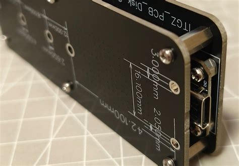
When assembling a PCB box build, understanding the interplay between design, component integration, and production workflows is critical This process involves more than just placing components on a board—it requires coordinating wiring harnesses, mechanical enclosures, and system-level testing to create a functional electronic device For PCB manufacturing companies, balancing pcb manufacturing cost with quality demands careful planning, especially when scaling production
Tip: Always validate enclosure dimensions early in the design phase to avoid costly rework during assembly.
A streamlined box build starts with selecting the right pcb manufacturing partner Key considerations include:
| Factor | In-House Assembly | Outsourced Assembly |
|---|---|---|
| Cost Control | Higher upfront investment | Predictable per-unit fees |
| Expertise Access | Limited to internal team | Leverage specialized skills |
| Scalability | Challenges in rapid scaling | Built for volume flexibility |
For instance, integrating custom wiring with pre-fabricated enclosures reduces assembly time, but requires precise alignment with the PCB layout Thermal management and vibration resistance often dictate material choices, impacting both durability and pcb manufacturing business margins
"A well-executed box build ensures reliability at every connection point," notes an industry veteran "Skip rigorous testing, and you risk field failures that dwarf initial savings."
To optimize pcb manufacturing cost, prioritize modular designs that simplify repairs and upgrades Partnering with pcb manufacturing companies that offer end-to-end services—from prototyping to final testing—can eliminate bottlenecks Remember: every minute saved in assembly translates to faster time-to-market for your product
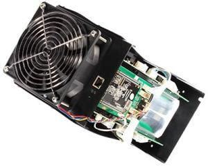
Integrating Wiring and Enclosures Efficiently
When designing PCB manufacturing systems, the interplay between wiring and enclosures directly impacts both functionality and scalability To achieve seamless integration, start by aligning design specifications with enclosure dimensions early in the planning phase PCB manufacturing companies often leverage 3D modeling tools to simulate component placement, ensuring optimal wire routing paths that avoid interference with structural elements like mounting brackets or ventilation ports This proactive approach minimizes rework and reduces PCB manufacturing cost by eliminating last-minute design adjustments
A critical step involves selecting materials that balance durability and thermal management For instance, using lightweight aluminum enclosures with pre-cut cable entry points simplifies wire harness installation while maintaining electromagnetic shielding Pairing this with modular wiring systems—such as ribbon cables or flexible printed circuits—allows for faster assembly and easier maintenance When working with PCB manufacturing business partners, confirm their capabilities in customizing enclosures for high-density layouts, as this ensures compatibility with complex PCB configurations
Automation plays a pivotal role here Robotic arms equipped with vision systems can precisely thread wires through tight spaces, reducing human error and accelerating throughput However, even automated processes require rigorous validation Implement real-time quality checks during enclosure assembly to detect misaligned connectors or pinched cables before final integration
Collaboration between mechanical and electrical teams is non-negotiable Regular cross-functional reviews help identify conflicts, such as a wire bundle obstructing a heat sink’s airflow By addressing these issues early, you streamline the entire PCB manufacturing workflow, ensuring enclosures and wiring systems work in harmony rather than competition This alignment not only cuts production delays but also fortifies product reliability—a cornerstone of competitive PCB manufacturing companies
Finally, consider scalability Standardizing connector types and enclosure footprints across product lines simplifies inventory management and future upgrades, directly benefiting your PCB manufacturing cost structure Whether prototyping or scaling, this integrated methodology ensures that wiring and enclosures evolve together, not as afterthoughts
Ensuring Reliability Through Rigorous Testing
To achieve dependable electronics manufacturing, rigorous testing protocols are non-negotiable When integrating wiring, enclosures, and components during PCB box build assembly, every connection and interface must withstand real-world stresses This begins with environmental stress screening (ESS), which exposes assemblies to extreme temperatures, vibrations, and humidity cycles By simulating harsh conditions early, you identify weaknesses in solder joints or component placements that could lead to field failures
Leading PCB manufacturing companies prioritize automated optical inspection (AOI) and in-circuit testing (ICT) to validate electrical performance AOI systems scan for physical defects like misaligned components or insufficient solder, while ICT checks continuity, resistance, and signal integrity These steps ensure that even subtle flaws—ones that might inflate PCB manufacturing cost through rework or recalls—are caught before final integration
For mission-critical applications, thermal cycling tests are essential Imagine a medical device PCB: repeated heating and cooling cycles verify that expansions and contractions won’t compromise connections over time Pair this with functional testing, where firmware and hardware interact under load, and you create a robust validation framework
Balancing thoroughness with efficiency is key Over-testing can delay timelines, while under-testing risks reliability Partnering with a PCB manufacturing business that employs statistical process control (SPC) helps optimize this balance By analyzing defect rates in real time, you refine testing phases to target high-risk areas without unnecessary repetition
Finally, documentation matters Traceability logs linked to each assembly stage ensure that if a failure occurs, root causes can be pinpointed swiftly This not only upholds quality but also builds trust with clients who depend on your PCB manufacturing expertise to deliver consistently safe, durable products
Optimizing Production Line Efficiency Strategies
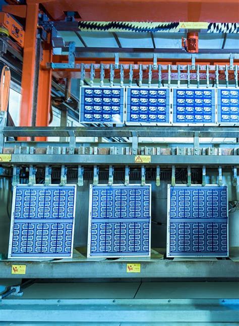
To achieve peak efficiency in PCB manufacturing, you must first analyze workflow bottlenecks that slow down assembly timelines Root causes often include manual component placement, inconsistent testing protocols, or disjointed communication between design and production teams By implementing automated pick-and-place systems paired with real-time process monitoring, PCB manufacturing companies can reduce human error while accelerating throughput by up to 40%
A lean approach to material handling further minimizes downtime For example, adopting just-in-time inventory management ensures components arrive precisely when needed, reducing storage costs and mitigating supply chain disruptions This is particularly critical when managing PCB manufacturing cost, as excess stock or delayed shipments directly impact profit margins Integrating IoT-enabled sensors into production lines also allows for predictive maintenance, identifying equipment wear before it leads to unplanned stoppages
Another strategy involves standardizing assembly protocols across all stages Modular workstations, where enclosures, wiring, and PCB integration occur in parallel, enable faster reconfiguration for different product batches When combined with digital twin simulations—a technique increasingly adopted by forward-thinking PCB manufacturing business leaders—you can test layout changes virtually, avoiding costly physical trial runs
Finally, cross-training technicians to handle multiple assembly stages ensures flexibility during demand surges Pairing this with data-driven KPIs, such as cycle time per unit or defect rates per station, creates accountability while highlighting areas for improvement By aligning these strategies, you not only streamline operations but also build a foundation for scalable growth in competitive electronics markets
Advanced Techniques for Streamlined Assembly
To achieve truly efficient PCB box build assembly, you need to adopt strategies that go beyond basic wiring and enclosure integration Modern PCB manufacturing relies on automated guided vehicles (AGVs) and robotic placement systems to minimize manual intervention, reducing errors while accelerating throughput For instance, pairing pcb manufacturing companies with advanced pick-and-place machines can cut assembly time by up to 40%, directly lowering pcb manufacturing cost and improving margins for your pcb manufacturing business
Modular design plays a pivotal role here By standardizing components like pre-fabricated cable harnesses or snap-fit enclosures, you eliminate guesswork during assembly This approach not only streamlines workflows but also ensures compatibility across product variants—a critical advantage when scaling operations Additionally, integrating design for manufacturability (DFM) principles early in the process helps identify potential bottlenecks, such as overly complex solder joints or misaligned mounting points, before they escalate into costly rework
Another game-changer is the use of real-time analytics to monitor production lines Sensors embedded in test fixtures can track metrics like torque consistency during screw fastening or thermal performance during power-on testing, flagging deviations instantly When combined with machine learning algorithms, these systems predict maintenance needs, further reducing downtime For example, one leading pcb manufacturing company reported a 25% drop in unplanned stoppages after implementing predictive analytics
Material selection also impacts efficiency Opting for lightweight, durable composites for enclosures simplifies handling while maintaining structural integrity—a balance that becomes vital in high-volume pcb manufacturing Meanwhile, adopting concurrent testing—where functional checks occur alongside assembly—slashes final inspection cycles This dual-phase verification ensures defects are caught early, aligning with rigorous quality benchmarks without slowing output
By weaving these techniques into your pcb manufacturing business, you create a cohesive assembly process where speed and precision coexist The result? A leaner operation that meets today’s demands for reliability without compromising scalability
Quality Control in Electronics Manufacturing
When integrating PCB manufacturing into your production workflow, maintaining rigorous quality control (QC) is non-negotiable Even minor defects in components or assembly can lead to costly recalls, damaged reputations, or safety hazards Leading PCB manufacturing companies implement multi-layered inspection protocols, starting with automated optical inspection (AOI) to detect soldering flaws or misaligned components This step ensures that every board meets design specifications before progressing to enclosure integration
Balancing PCB manufacturing cost with reliability requires strategic testing at critical stages For instance, functional testing under simulated operating conditions—such as thermal cycling or vibration tests—helps identify weaknesses in wiring harnesses or connector durability By catching issues early, you avoid compounding errors in later phases, which could derail timelines and inflate expenses Advanced traceability systems also play a pivotal role, enabling precise tracking of components back to their suppliers This is especially vital for PCB manufacturing businesses handling high-mix, low-volume orders where material consistency is key
To optimize QC further, consider adopting statistical process control (SPC) methods By analyzing real-time data from assembly lines, you can pinpoint variability in solder paste application or component placement accuracy Pairing this with failure mode and effects analysis (FMEA) creates a proactive framework for mitigating risks For example, moisture-sensitive components might require controlled storage environments to prevent oxidation, a common culprit in field failures
Ultimately, robust QC isn’t just about compliance—it’s about building trust When end-users receive products that perform flawlessly under stress, it reinforces the value of partnering with PCB manufacturing experts who prioritize precision at every step
Custom Solutions for Diverse Box Build Needs
When addressing PCB box build assembly, one size rarely fits all Your project might demand specialized configurations based on industry standards, environmental conditions, or unique performance criteria For instance, high-density wiring for aerospace applications requires precision that differs starkly from ruggedized enclosures needed in industrial automation This variability is where partnering with experienced PCB manufacturing companies becomes critical These providers analyze your requirements—whether it’s optimizing PCB manufacturing cost for consumer electronics or ensuring compliance with medical-grade safety protocols—to deliver tailored solutions that align with your technical and budgetary constraints
A key advantage of custom box builds lies in scalability Startups in the PCB manufacturing business often prioritize modular designs that allow incremental upgrades, while established enterprises might focus on fully integrated systems for mass production Advanced providers employ design-for-manufacturability (DFM) principles to simplify complex assemblies, reducing material waste and assembly time For example, integrating pre-tested cable harnesses or pre-configured enclosure layouts can accelerate deployment without compromising reliability
Cost optimization doesn’t end with design Leading manufacturers leverage value engineering to identify alternatives—such as lightweight composite enclosures or automated testing protocols—that maintain performance while lowering PCB manufacturing cost This approach is particularly valuable for industries like renewable energy, where durability and affordability are equally critical
Finally, flexibility extends to post-production support Whether you need localized inventory management for global distribution or firmware updates for IoT-enabled devices, a collaborative partnership ensures your PCB box build evolves alongside market demands By aligning with providers that offer both technical expertise and agile workflows, you create a foundation for innovation without sacrificing quality or efficiency
End-to-End Integration for Seamless Production
Achieving seamless production in PCB manufacturing requires synchronizing every stage of the assembly process, from design validation to final product testing By integrating design software, automated assembly tools, and quality assurance protocols into a unified workflow, PCB manufacturing companies can eliminate bottlenecks that delay timelines or compromise reliability For instance, pairing CAD files with automated pick-and-place systems ensures component placement accuracy, while real-time data sharing between teams prevents mismatches between enclosure specifications and PCB dimensions
A critical advantage of end-to-end integration lies in reducing PCB manufacturing cost Automated material tracking systems minimize waste by precisely calculating component requirements, while predictive maintenance algorithms prevent costly equipment downtime Lean manufacturing principles further enhance efficiency by streamlining workflows—such as combining wiring harness assembly with enclosure mounting in a single station This approach not only accelerates throughput but also ensures consistency, particularly when scaling production for high-volume orders
For businesses managing a PCB manufacturing business, end-to-end integration also simplifies compliance with industry standards Embedded testing protocols, like in-circuit and functional testing, validate each unit’s performance before it leaves the production line By centralizing data from these tests, manufacturers gain actionable insights to refine processes proactively Additionally, cloud-based collaboration platforms enable seamless communication between engineers, suppliers, and clients, ensuring design changes are implemented without disrupting timelines
Ultimately, the goal is to create a self-optimizing ecosystem where design, assembly, and testing operate as interdependent components rather than isolated steps This holistic approach not only elevates product quality but also positions PCB manufacturing enterprises to adapt swiftly to evolving market demands—whether scaling production or customizing solutions for niche applications
Conclusion
As you refine your approach to PCB box build assembly, the integration of design, testing, and production becomes pivotal for delivering reliable electronics Partnering with experienced PCB manufacturing companies ensures that every component—from wiring harnesses to enclosures—aligns with your project’s technical and budgetary requirements Cost efficiency remains a critical factor, but cutting corners in PCB manufacturing cost should never compromise the integrity of the final product Instead, focus on optimizing material selection and assembly workflows to balance affordability with performance
For businesses scaling their PCB manufacturing business, adopting advanced automation and modular design principles can significantly reduce assembly time while maintaining consistency Rigorous quality checks, such as automated optical inspections and functional testing, act as safeguards against defects, ensuring that each unit meets industry standards This end-to-end oversight not only minimizes rework but also builds trust with clients who depend on durable, high-performance solutions
Customization plays a vital role in addressing diverse application needs Whether you’re producing consumer electronics or industrial control systems, tailoring enclosure designs and component layouts ensures compatibility with specific operational environments By leveraging scalable PCB manufacturing processes, you can adapt to fluctuating demand without sacrificing precision or lead times
Ultimately, the success of your box build project hinges on seamless collaboration between design, assembly, and testing teams Prioritizing traceability and documentation at every stage creates a transparent workflow, enabling quick troubleshooting and continuous improvement As the electronics industry evolves, staying ahead requires not just technical expertise but a commitment to innovation in PCB manufacturing practices
Frequently Asked Questions
How does prototyping affect PCB box build assembly timelines?
Prototyping allows you to verify design integrity before full-scale production, reducing risks of delays Early-stage testing with PCB manufacturing partners ensures enclosures, wiring, and component layouts meet specifications, streamlining the transition to mass production
What factors influence PCB manufacturing cost for complex box builds?
Costs depend on material selection, assembly complexity, and testing requirements High-density interconnects, custom enclosures, and rigorous quality validation processes may increase expenses Partnering with experienced PCB manufacturing companies helps optimize budgets through design-for-manufacturability (DFM) analysis
Can existing enclosures be reused for new PCB box builds?
While possible, compatibility depends on dimensional tolerances and thermal management needs Redesigning enclosures often becomes necessary when upgrading components or integrating advanced features Collaborate with your PCB manufacturing business provider to assess retrofitting feasibility versus new builds
How do you ensure reliability in high-volume box build production?
Implement automated optical inspection (AOI) and functional testing at every stage Reputable PCB manufacturing suppliers combine these checks with traceability systems to monitor yield rates and identify defects early Regular audits of solder joints and wiring harnesses further enhance consistency
What certifications should PCB manufacturing companies hold for medical/industrial box builds?
Look for ISO 13485 (medical devices) or ISO 9001 (industrial systems), alongside UL/CE compliance These standards validate adherence to safety protocols and production rigor, critical for applications requiring zero-failure tolerance
How do PCB manufacturing partners address supply chain disruptions?
Leading providers diversify component sourcing, maintain buffer inventories, and leverage predictive analytics to mitigate shortages Supplier transparency and real-time inventory dashboards help you adjust timelines proactively
Ready to Optimize Your Box Build Assembly?
For tailored solutions that balance PCB manufacturing cost and quality, please click here to consult experts specializing in end-to-end electronics production


