Streamlining PCB Fabrication & Assembly Service Processes

Key Takeaways
Effective PCB fabrication and assembly processes rely on balancing speed, precision, and scalability. By integrating PCBA-specific automation tools, manufacturers reduce human error while accelerating PCB assembly timelines. Advanced techniques like automated optical inspection (AOI) and surface-mount technology (SMT) ensure consistent quality, even in high-volume orders. For prototyping, modular workflows enable rapid iteration without compromising cost-efficiency, while bulk production benefits from optimized material sourcing and standardized testing protocols.
Crucially, design for manufacturability (DFM) checks streamline workflows by identifying potential bottlenecks early, minimizing rework. Modern PCB fabrication services also leverage real-time data analytics to refine process parameters, ensuring tighter tolerances and higher yield rates. Additionally, partnerships with certified suppliers for components like high-density interconnects (HDIs) enhance reliability across PCBA stages.
To maintain competitiveness, manufacturers must adopt agile frameworks that align PCB assembly timelines with dynamic project demands. This includes flexible scheduling for mixed-batch orders and scalable quality assurance systems. By prioritizing these strategies, businesses achieve faster turnaround, reduced waste, and seamless transitions from prototyping to mass production—key drivers in today’s fast-paced electronics market.
Optimizing PCB Fabrication Speed
Achieving faster PCB fabrication cycles requires a strategic balance between process automation, material selection, and design optimization. Modern facilities leverage automated optical inspection (AOI) systems to reduce manual checks, accelerating production while maintaining accuracy. For instance, integrating PCBA workflows with advanced CAD/CAM software minimizes design-to-production delays by identifying potential errors early.
| Factor | Traditional Approach | Optimized Approach |
|---|---|---|
| Design Verification | Manual review | AI-driven analysis |
| Material Handling | Batch processing | Just-in-time (JIT) |
| Assembly Alignment | Manual placement | Robotic pick-and-place |
"Speed in PCB manufacturing isn’t just about machinery—it’s about synchronizing every stage, from prototyping to PCB assembly, to eliminate bottlenecks." – Industry Expert
Using high-density interconnect (HDI) substrates and laser-drilled microvias can significantly shorten fabrication timelines for complex designs. Additionally, partnering with suppliers offering fast-turn materials ensures consistent availability, avoiding production halts. A critical tip for designers:
Standardize component footprints in your CAD libraries to simplify PCBA workflows and reduce setup time during mass production.
By aligning design specifications with fabrication capabilities, manufacturers can achieve 30-50% faster turnaround without compromising quality. This approach is particularly impactful for high-mix, low-volume projects where rapid iteration defines market competitiveness.
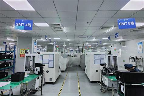
Advanced PCB Assembly Techniques
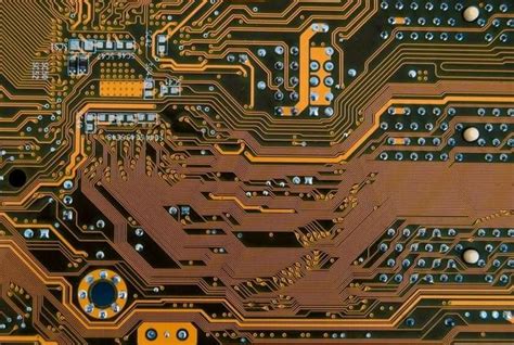
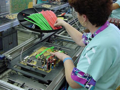
Modern PCB assembly processes leverage cutting-edge methodologies to balance speed, accuracy, and scalability. Central to this evolution is the integration of automated optical inspection (AOI) systems, which meticulously scan PCBA boards for defects like misaligned components or solder bridging. These systems minimize human error while enabling real-time corrections, ensuring compliance with stringent quality benchmarks. Additionally, surface-mount technology (SMT) has revolutionized component placement, allowing for ultra-high-density layouts that meet the demands of compact, high-performance electronics.
To further enhance precision, manufacturers now employ laser-direct imaging (LDI) for creating intricate circuit patterns with micron-level accuracy. This technique reduces reliance on traditional photomasks, accelerating prototyping cycles without compromising resolution. For complex assemblies, selective soldering ensures reliable connections in mixed-technology boards, particularly where through-hole and SMT components coexist.
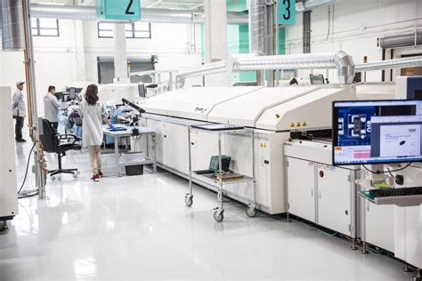
Scalability remains a priority, with modular PCB assembly lines enabling seamless transitions between low-volume prototyping and high-volume production. Advanced thermal profiling optimizes reflow soldering processes, preventing warping or delamination in temperature-sensitive materials. By integrating these innovations, PCBA providers achieve faster turnaround times while maintaining consistent output quality—a critical advantage in industries requiring rapid iteration, such as IoT devices or automotive systems.
The adoption of intelligent traceability systems further strengthens process control, tracking each component from procurement to final testing. This not only streamlines compliance with regulatory standards but also supports rapid root-cause analysis during quality audits. Together, these techniques underscore how modern PCB assembly solutions are redefining efficiency in electronics manufacturing.
Cost-Effective PCB Prototyping Solutions
Achieving affordability in PCB prototyping requires a strategic balance between design optimization, material selection, and advanced manufacturing techniques. By leveraging automated design validation tools, engineers can identify potential inefficiencies early, minimizing costly revisions. Modern PCB assembly (PCBA) workflows integrate high-speed pick-and-place systems and precision soldering technologies, enabling rapid iteration without compromising quality. For startups and R&D teams, partnering with specialized providers like Fineline Circuits ensures access to scalable prototyping solutions that align with budget constraints.
Material efficiency plays a critical role: opting for standardized substrate sizes and multilayer stacking reduces waste, while modular PCBA designs allow reusable components across prototypes. Advanced quoting platforms further streamline cost estimation, offering real-time adjustments based on design complexity and volume. For projects transitioning from prototyping to mass production, adopting design-for-manufacturability (DFM) principles ensures seamless scaling, avoiding costly redesigns. This approach not only accelerates time-to-market but also establishes a foundation for consistent quality in subsequent bulk PCB assembly phases.
Precision in PCB Manufacturing Processes
Achieving precision in PCB fabrication requires meticulous attention to detail across design, material selection, and production stages. Advanced technologies such as automated optical inspection (AOI) and laser direct imaging (LDI) ensure micron-level accuracy in circuit patterning, minimizing deviations that could compromise functionality. For PCB assembly (PCBA), precise solder paste application and component placement are critical, particularly in high-density designs where even minor misalignments can lead to failures.
Modern PCBA workflows leverage robotic pick-and-place systems paired with real-time monitoring to maintain tolerances as tight as ±0.01mm. Additionally, temperature-controlled reflow ovens and conformal coating processes enhance reliability by preventing thermal stress and environmental damage. Material consistency also plays a pivotal role; using low-loss dielectrics and high-purity copper substrates reduces signal attenuation in high-frequency applications.
To sustain precision at scale, manufacturers implement statistical process control (SPC), analyzing data from each production batch to identify and correct variances early. This approach not only aligns with stringent PCB fabrication standards but also supports seamless integration with downstream assembly stages, ensuring end-to-end quality. By harmonizing cutting-edge tools with rigorous quality protocols, the industry delivers repeatable accuracy across prototyping and mass production, meeting the demands of sectors like aerospace and medical electronics.

Bulk PCB Assembly Efficiency Strategies
Achieving optimal efficiency in PCB assembly for large-scale production requires strategic planning and process refinement. Manufacturers implementing high-volume PCBA workflows often leverage automated pick-and-place systems to minimize human error while accelerating component placement. Pairing this with real-time monitoring tools ensures consistent throughput, even during extended production runs. For instance, integrating advanced optical inspection (AOI) at critical checkpoints reduces post-assembly defects, aligning with the demand for precision in bulk orders.
Another key strategy involves standardizing component libraries to streamline design-for-manufacturing (DFM) reviews. By pre-validating commonly used parts, teams reduce revision cycles and accelerate time-to-market. Additionally, adopting just-in-time (JIT) inventory models for materials minimizes storage costs and mitigates supply chain disruptions—a critical factor for cost-effective PCB assembly at scale.
Collaborative planning with suppliers further enhances efficiency. Establishing shared production schedules and automated order-tracking systems ensures seamless coordination between fabrication and assembly phases. This approach not only supports rapid scaling but also maintains flexibility for last-minute design adjustments, a necessity in dynamic manufacturing environments. By prioritizing these strategies, businesses can achieve faster turnaround without compromising the reliability of high-volume PCBA outputs.
Streamlined PCB Production Workflows
Modern PCB fabrication and assembly processes thrive on integrated workflows that eliminate redundancies between design, manufacturing, and testing. By synchronizing PCB assembly (PCBA) stages with fabrication protocols, manufacturers reduce idle time between production phases. Automated optical inspection (AOI) systems and machine-learning-driven defect detection ensure seamless transitions from bare-board fabrication to component placement, minimizing manual interventions.
Centralized data management platforms further optimize workflow efficiency, enabling real-time tracking of PCBA orders across global supply chains. For instance, collaborating with a PCB manufacturer’s representative can align design specifications with production capabilities early in the process, avoiding costly revisions. Advanced design-for-manufacturability (DFM) tools also preempt bottlenecks by flagging potential assembly issues during the prototyping phase.
Modular assembly lines, tailored for both low-volume and high-mix orders, enhance adaptability without compromising speed. This approach ensures consistent quality while scaling from prototype validation to bulk production. By embedding just-in-time inventory practices and lean manufacturing principles, streamlined workflows deliver cost-effective PCB assembly solutions with lead times reduced by up to 30% compared to traditional methods. Such optimizations underscore the strategic value of unifying fabrication and assembly under a cohesive operational framework.
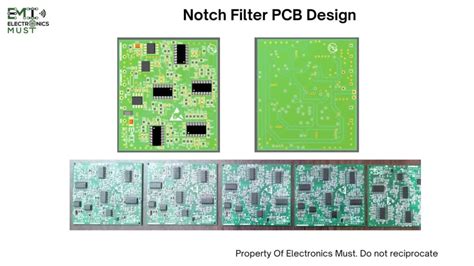
Enhancing PCB Fabrication Quality Standards
Modern PCB fabrication relies on rigorous quality control protocols to meet the escalating demands of electronics manufacturing. Implementing automated optical inspection (AOI) systems ensures microscopic defect detection in PCB assembly layers, while X-ray inspection validates internal connections in multilayer boards. These technologies work synergistically to identify issues like solder voids or misaligned traces early, reducing rework costs and delays.
Material selection plays a pivotal role in quality enhancement. High-grade substrates with low dielectric loss and thermal stability minimize signal degradation, particularly in high-frequency applications. For PCBA processes, advanced solder paste formulations and precision stencil printing enable consistent component placement, critical for fine-pitch ICs and BGAs.
Collaboration with certified partners, such as RP Electronics, ensures adherence to ISO 9001 and IPC-A-610 standards. Their expertise in design-for-manufacturing (DFM) analysis optimizes layouts for both fabrication and PCB assembly, preventing flaws like copper imbalance or insufficient clearance.
Finally, real-time monitoring of environmental conditions—humidity, temperature, and particulate levels—maintains production integrity. Combined with statistical process control (SPC), these measures elevate yield rates while supporting scalable solutions from prototyping to mass production. This holistic approach bridges quality and efficiency, aligning with evolving industry benchmarks for reliability and performance.
Rapid PCB Mass Production Innovations
Modern advancements in PCB assembly technologies are revolutionizing high-volume manufacturing, enabling faster scaling without compromising precision. Automated pick-and-place systems, combined with high-speed surface-mount technology (SMT), reduce placement errors while accelerating throughput by up to 40%. For PCBA projects, dual-lane production lines and modular workflows allow simultaneous processing of multiple batches, slashing lead times for bulk orders. Real-time monitoring tools, such as automated optical inspection (AOI), ensure consistent quality across thousands of units by detecting defects early in the assembly cycle.
To further optimize efficiency, manufacturers like Rocket PCB integrate AI-driven predictive maintenance, minimizing downtime during PCB fabrication. Advanced panelization techniques maximize material utilization, reducing waste and costs for large-scale runs. Additionally, laser-direct imaging (LDI) systems enhance trace accuracy in high-density interconnect (HDI) designs, critical for applications like IoT and automotive electronics. These innovations not only support rapid scaling but also maintain alignment with stringent industry compliance standards, ensuring reliability from prototyping to full-scale production.
Conclusion
The evolution of PCB assembly processes underscores the importance of integrating precision-driven methodologies with scalable workflows to meet modern manufacturing demands. By leveraging advanced PCBA technologies—such as automated pick-and-place systems and AI-driven quality control—companies can achieve faster turnaround times while maintaining stringent quality standards. This approach not only reduces material waste but also ensures seamless transitions from prototyping to high-volume production.
A critical factor in optimizing PCB fabrication and assembly services lies in adopting modular workflows that adapt to both small-batch and bulk requirements. For instance, integrating box-build assembly techniques further enhances end-to-end efficiency by consolidating component integration stages. Such strategies minimize delays and enable manufacturers to address dynamic market needs without compromising on cost-effectiveness or reliability.
Ultimately, the synergy between PCB assembly innovation and process standardization creates a foundation for sustainable growth. By prioritizing data-driven decision-making and continuous improvement, stakeholders across industries can unlock new levels of operational agility, ensuring their products remain competitive in an increasingly fast-paced technological landscape.

FAQs
How does streamlined PCB assembly improve production timelines?
By integrating automated PCBA processes and optimized material logistics, manufacturers reduce manual interventions, accelerating both prototyping and bulk production phases. Advanced scheduling algorithms further minimize downtime between fabrication stages.
What cost factors should be considered for PCB prototyping?
Key considerations include material selection, layer count, and testing protocols. Economical PCB assembly often leverages standardized components and panelization techniques to lower per-unit costs without compromising precision.
How is precision maintained in high-volume PCBA workflows?
Automated optical inspection (AOI) systems and real-time quality monitoring ensure consistent solder joint integrity and component alignment. These systems complement PCB fabrication tolerances as tight as ±0.05mm for critical applications.
Can bulk orders accommodate custom design revisions?
Yes, modern PCB assembly services employ flexible manufacturing cells that allow mid-production adjustments. This agility supports iterative improvements while maintaining cost efficiency across 1,000+ unit batches.
What distinguishes turnkey PCBA from conventional services?
Turnkey solutions consolidate PCB fabrication, component sourcing, and testing into a single workflow, eliminating vendor coordination delays. This approach typically reduces total project timelines by 30–40% compared to fragmented service models.
Ready to Optimize Your PCB Production?
Explore our advanced PCBA solutions tailored for rapid scaling and precision engineering. Click here to request a customized quote or discuss your project requirements with our technical team.