Streamlining PCB Production: Modern Manufacturing Strategies

Key Takeaways
When navigating the complexities of PCB manufacturing, understanding how modern strategies impact your operations is critical Today’s PCB manufacturing companies leverage smart manufacturing systems to balance PCB manufacturing cost with precision and scalability For instance, automated optical inspection (AOI) and AI-driven defect detection reduce human error, directly lowering rework expenses—a key concern for any PCB manufacturing business
Consider the following cost comparison between traditional and modern approaches:
| Factor | Traditional Methods | Modern Strategies |
|---|---|---|
| Defect Detection Rate | 85-90% | 98-999% |
| Time-to-Market | 8-12 weeks | 4-6 weeks |
| Cost per Unit (High-Volume) | $250-$300 | $180-$220 |
By adopting data-driven workflows, you can optimize material usage and minimize waste, which accounts for up to 15% of PCB manufacturing cost in legacy systems For example, predictive maintenance tools extend equipment lifespan, reducing downtime by 30-40%—a game-changer for maintaining profit margins
Sustainability is another pillar reshaping the industry Leading PCB manufacturing companies now prioritize closed-loop water recycling and halogen-free materials, aligning with global regulations while appealing to eco-conscious clients These practices not only future-proof your PCB manufacturing business but also create differentiated value in competitive markets
Finally, integrating AI-driven analytics enables real-time adjustments during production Imagine dynamically recalibrating etching parameters based on live sensor data—this level of agility ensures consistent quality even for high-density interconnect (HDI) designs As you refine your approach, remember: balancing innovation with cost-efficiency isn’t optional; it’s the backbone of thriving in modern PCB manufacturing

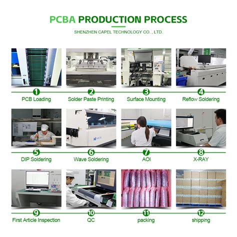
Smart Manufacturing in PCB Assembly
Adopting smart manufacturing in PCB assembly transforms how pcb manufacturing companies approach production cycles By integrating IoT-enabled sensors and machine learning algorithms, you gain real-time visibility into equipment performance, material flow, and defect patterns This shift reduces pcb manufacturing cost by minimizing scrap rates—studies show smart factories achieve up to 30% less material waste compared to traditional setups
For instance, predictive maintenance systems analyze vibration and temperature data from pick-and-place machines, alerting technicians before component misalignment disrupts assembly lines This proactive approach ensures consistent output quality while optimizing machine uptime—a critical advantage in high-volume pcb manufacturing business operations
The integration of digital twin technology further refines process control By creating virtual replicas of physical assembly lines, you simulate layout adjustments or throughput changes without halting production This capability becomes vital when balancing pcb manufacturing timelines with custom client specifications, particularly in aerospace or medical device applications where tolerance thresholds are stringent
Automated optical inspection (AOI) systems, powered by deep learning vision algorithms, now detect micron-level soldering defects that human inspectors might miss When paired with closed-loop feedback mechanisms, these systems automatically recalibrate soldering irons or stencil printers, creating self-optimizing workflows Such innovations not only elevate reliability but also compress lead times—key for businesses competing in fast-turn pcb manufacturing markets
However, implementing smart systems requires strategic planning While upfront investments in edge computing infrastructure or 5G-enabled factories impact short-term pcb manufacturing cost, the long-term ROI manifests through accelerated prototyping cycles and reduced rework expenses Leading pcb manufacturing companies report 18–22% faster time-to-market after digitizing their assembly floors, proving that intelligent automation isn’t just an option—it’s the new baseline for competitiveness
Precision Engineering for PCB Reliability
Achieving consistent reliability in PCB manufacturing requires a meticulous focus on precision engineering principles When designing circuit boards, you’re not just arranging copper traces—you’re building the foundation for electronic systems that must perform flawlessly under thermal stress, vibration, and prolonged use Leading PCB manufacturing companies employ advanced techniques like laser direct imaging (LDI) and automated optical inspection (AOI) to ensure micron-level accuracy in trace alignment and via placement These methods minimize defects that could compromise signal integrity or lead to premature failures
A critical factor in balancing PCB manufacturing cost and quality lies in material selection High-performance substrates like polyimide or FR-4 with low dielectric loss are chosen based on application-specific requirements For instance, aerospace or medical devices demand materials that withstand extreme temperatures, while consumer electronics prioritize cost-efficiency By simulating thermal and mechanical stresses during the design phase, engineers can predict failure points and optimize layouts before prototyping—saving time and reducing waste in the PCB manufacturing business
To further enhance reliability, modern manufacturers integrate design-for-manufacturability (DFM) checks directly into their workflows This proactive approach identifies potential issues like insufficient solder mask clearance or uneven copper distribution early in the process Partnering with experienced providers like Andwin PCB ensures access to these precision-driven methodologies, which are essential for producing boards that meet stringent industry standards
The shift toward miniaturization in electronics adds another layer of complexity Microvia drilling and sequential lamination techniques enable higher-density interconnects without sacrificing durability By combining these innovations with rigorous testing protocols—such as thermal cycling and accelerated aging—you create products that deliver long-term performance even in harsh operating environments This strategic alignment of engineering precision and quality control transforms reliability from a passive outcome into a measurable competitive advantage

Optimizing PCB Workflow Efficiency
To achieve peak efficiency in PCB manufacturing, you need to rethink how design, prototyping, and production stages interact Modern PCB manufacturing companies leverage digital twin simulations to identify bottlenecks before physical production begins By mapping workflows in virtual environments, you can test layout adjustments, material substitutions, or equipment reconfigurations without disrupting active production lines
A critical step is integrating automated design-for-manufacturing (DFM) checks directly into your CAD software These tools flag potential issues like insufficient trace spacing or thermal hotspots, reducing post-prototype revisions by up to 40% For example, pairing DFM validation with real-time collaboration platforms allows engineers and fabricators to resolve conflicts during the design phase rather than after costly prototypes are built
Pro Tip: Use predictive analytics to forecast PCB manufacturing cost fluctuations Machine learning models trained on historical data can alert you to price spikes in substrates or copper cladding, enabling proactive supplier negotiations
Another focus area is streamlining material handling PCB manufacturing business workflows often lose efficiency through manual component sorting or inventory mismatches Implementing RFID-tagged reel tracking systems ensures precise material usage monitoring, while automated storage/retrieval systems (AS/RS) cut retrieval times by 65% For high-mix production, dynamic scheduling algorithms adjust machine priorities based on real-time order changes, minimizing idle tooling time
Finally, adopt closed-loop feedback between quality control and process engineering When automated optical inspection (AOI) systems detect recurring defects, that data should trigger immediate calibration updates in solder paste dispensers or pick-and-place machines This self-correcting workflow not only reduces scrap rates but also accelerates yield improvements across batches
Advanced PCB Prototyping Techniques
When transitioning from design to functional boards, PCB manufacturing relies on prototyping methods that balance speed, accuracy, and scalability Modern design validation processes now integrate additive manufacturing, such as 3D-printed circuit layers, to reduce pcb manufacturing cost by up to 40% compared to traditional etching Leading pcb manufacturing companies leverage AI-driven simulation tools to predict signal integrity issues early, minimizing costly redesign cycles For instance, impedance-matching algorithms can automatically adjust trace geometries in multilayer boards before physical production begins
Rapid prototyping isn’t just about speed—it’s about creating a feedback loop between engineers and fabrication teams By using laser-direct imaging (LDI) systems, you can achieve micron-level alignment accuracy, critical for high-density interconnect (HDI) designs This precision directly impacts the pcb manufacturing business by enabling smaller batch runs without compromising quality—ideal for IoT devices or medical electronics Hybrid workflows, combining automated optical inspection (AOI) with real-time data analytics, further streamline iterations, cutting development timelines by 25–35%
To optimize pcb manufacturing efficiency, consider modular prototyping platforms that support flexible material choices For example, high-frequency laminates or flexible substrates can be tested alongside standard FR-4 boards within the same production queue This approach lets you validate performance under varied conditions while maintaining cost control Advanced firms even employ digital twins—virtual replicas of physical boards—to simulate thermal behavior and EMI risks before committing to full-scale production
The shift toward smarter prototyping also addresses sustainability Water-soluble solder masks and additive processes reduce chemical waste, aligning with eco-conscious regulations without inflating pcb manufacturing cost By adopting these techniques, you position your pcb manufacturing business to meet both technical demands and environmental standards, ensuring competitiveness in an industry where agility and precision define success
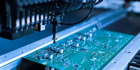
Automation in Circuit Board Production
The integration of automation into PCB manufacturing is redefining how precision and speed converge in electronics production By deploying robotic assembly lines and AI-guided inspection systems, PCB manufacturing companies minimize human intervention while maximizing consistency—critical for meeting today’s demand for high-reliability circuit boards For instance, automated pick-and-place machines achieve micron-level accuracy, reducing errors in component positioning by over 90% compared to manual methods
Beyond efficiency gains, automation directly addresses PCB manufacturing cost challenges While initial investments in automated machinery may seem steep, they slash long-term expenses by cutting material waste and rework rates A single robotic system can handle tasks equivalent to 10–15 technicians, streamlining labor costs without compromising output quality This scalability is particularly advantageous for PCB manufacturing business models targeting high-volume orders or rapid prototyping cycles
Smart workflow integration further enhances these systems Automated optical inspection (AOI) tools, paired with machine learning algorithms, detect defects like soldering flaws or trace misalignments in real time—ensuring issues are flagged before boards advance to testing phases This proactive approach not only accelerates production but also aligns with stringent quality standards demanded by industries such as aerospace and medical devices
However, balancing automation with flexibility remains key Advanced systems now support quick-change tooling and modular setups, allowing manufacturers to pivot between product designs without lengthy downtime For smaller PCB manufacturing companies, hybrid models—combining automated processes with selective manual oversight—offer a cost-effective entry point into modernized production
As you evaluate automation strategies, consider how these technologies align with your operational scale and complexity Whether optimizing for PCB manufacturing cost reduction or preparing for future AI-driven expansions, the right automated infrastructure can future-proof your production pipeline while maintaining competitive agility
Quality Control in Modern PCB Manufacturing
In today’s competitive landscape, maintaining rigorous quality control standards is non-negotiable for PCB manufacturing companies aiming to deliver reliable products Modern systems now integrate automated optical inspection (AOI) and X-ray testing to detect microscopic defects in multilayer boards, ensuring every circuit aligns with design specifications These technologies minimize human error while accelerating inspection cycles—a critical advantage when balancing PCB manufacturing cost and throughput
You’ll find that leading manufacturers employ statistical process control (SPC) to monitor production variables in real time By analyzing data from solder paste application to final etching, they identify deviations before they escalate into costly rework For instance, temperature fluctuations during lamination can compromise dielectric properties, but IoT-enabled sensors now trigger instant adjustments, preserving material integrity This proactive approach not only safeguards product quality but also stabilizes long-term PCB manufacturing business margins by reducing scrap rates
Another game-changer is the adoption of artificial intelligence for predictive maintenance By training algorithms on historical failure patterns, equipment downtime drops by up to 40%, directly impacting production schedules and client satisfaction Meanwhile, cross-functional teams use digital twin simulations to stress-test designs under virtual conditions, catching potential flaws long before physical prototyping begins
While advanced tools elevate standards, compliance remains rooted in certifications like ISO 9001 and IPC-A-600 Regular audits ensure that even as automation expands, every layer of the PCB manufacturing process adheres to globally recognized benchmarks After all, in an industry where a single faulty via can halt an entire assembly line, precision isn’t just a goal—it’s the foundation of trust between manufacturers and their clients

Sustainable Practices in PCB Fabrication
Adopting eco-conscious methods in pcb manufacturing isn’t just an environmental obligation—it’s a strategic advantage Leading pcb manufacturing companies now prioritize closed-loop systems that recover copper from etching waste and reuse process water, reducing both resource consumption and pcb manufacturing cost By integrating biodegradable solder masks and halogen-free substrates, you minimize hazardous byproducts while maintaining performance standards
Energy efficiency plays a pivotal role in modern sustainability frameworks Factories are transitioning to renewable energy sources like solar or wind power, cutting operational emissions by up to 40% Advanced thermal management systems in high-density interconnect (HDI) production further optimize energy use, aligning with global carbon neutrality goals For your pcb manufacturing business, this not only lowers utility expenses but also strengthens compliance with regulations like RoHS and REACH
Waste reduction strategies extend beyond materials Predictive analytics tools monitor production lines in real time, identifying inefficiencies that lead to scrap By implementing lean manufacturing principles, you can achieve near-zero-defect outputs, ensuring fewer boards are discarded during quality checks Some innovators even repurpose defective PCBs into raw materials for low-cost prototypes, creating circular economies within their supply chains
Collaboration across the value chain amplifies these efforts Partnering with suppliers who provide conflict-free minerals or recycled laminates reinforces sustainability commitments For end users, transparent reporting on carbon footprints and recyclability metrics builds trust and differentiates your services in competitive markets
Balancing ecological responsibility with pcb manufacturing cost requires careful planning, but the long-term payoff—enhanced brand loyalty, regulatory resilience, and operational savings—makes it a cornerstone of future-ready fabrication strategies
AI-Driven PCB Production Systems
When optimizing PCB manufacturing workflows, integrating artificial intelligence (AI) unlocks transformative efficiencies that directly address challenges like pcb manufacturing cost and production scalability Modern pcb manufacturing companies leverage AI to analyze vast datasets from design, assembly, and testing phases, identifying patterns that human operators might overlook For example, machine learning algorithms predict equipment maintenance needs, reducing unplanned downtime by up to 30% in high-volume production environments Real-time defect detection systems, powered by computer vision, scan boards at micron-level precision, minimizing rework and material waste—a critical advantage for businesses aiming to balance pcb manufacturing business growth with sustainability goals
AI also refines design-for-manufacturability (DFM) processes By simulating thousands of design iterations under varying thermal, mechanical, and electrical conditions, generative AI tools propose layouts that optimize material usage and signal integrity This not only accelerates prototyping but ensures designs align with pcb manufacturing cost constraints without compromising reliability Automated routing algorithms further streamline trace placement, cutting engineering hours by 40–60% compared to manual methods
For pcb manufacturing companies transitioning to smart factories, AI-driven demand forecasting adjusts production schedules dynamically, aligning inventory levels with market fluctuations This agility is particularly valuable in industries like automotive or IoT, where component shortages or sudden order spikes can disrupt traditional workflows By implementing AI, manufacturers transform raw data into actionable insights, creating a competitive edge in an increasingly fast-paced electronics landscape
Conclusion
As you navigate the evolving landscape of PCB manufacturing, it becomes clear that success hinges on balancing innovation with practicality Modern strategies—from AI-driven automation to precision engineering—are reshaping how PCB manufacturing companies deliver reliable, high-performance circuit boards By integrating smart systems, you not only optimize production workflows but also address critical challenges like PCB manufacturing cost and time-to-market pressures
The shift toward sustainability and data-driven decision-making underscores a broader industry transformation For instance, adopting energy-efficient processes or recyclable materials isn’t just an ethical choice—it’s a competitive differentiator that aligns with global regulatory standards Similarly, leveraging real-time analytics helps identify bottlenecks in your PCB manufacturing business, enabling proactive adjustments that minimize waste and maximize output
However, the true value of these advancements lies in their scalability Whether you’re prototyping or scaling mass production, modular automation systems allow you to adapt quickly to fluctuating demands without compromising quality This flexibility is particularly vital when balancing custom client requirements with cost-efficiency targets
Ultimately, the future of PCB manufacturing depends on continuous innovation By staying ahead of trends like AI-powered defect detection or collaborative robotics, you position your operations to meet the ever-growing demands of industries reliant on advanced electronics The key is to view these technologies not as isolated tools but as interconnected components of a holistic manufacturing ecosystem—one where precision, speed, and sustainability coexist seamlessly
Frequently Asked Questions
How does automation impact pcb manufacturing costs in high-volume production?
Automation reduces pcb manufacturing expenses by minimizing human error and accelerating throughput Advanced pick-and-place systems and automated optical inspection (AOI) cut labor costs while improving yield rates, making large-scale production economically viable for pcb manufacturing companies
What qualifications should I prioritize when selecting pcb manufacturing companies?
Look for ISO-certified partners with expertise in high-density interconnect (HDI) designs and flexible PCB fabrication Reputable pcb manufacturing businesses often provide design-for-manufacturability (DFM) feedback, ensuring your prototypes align with scalable production workflows
Can sustainable practices lower long-term pcb manufacturing costs?
Yes Recycling copper cladding, adopting lead-free finishes, and optimizing panel utilization reduce material waste Many pcb manufacturing facilities now use energy-efficient curing ovens, which trim operational expenses while meeting environmental regulations
How do AI-driven systems enhance quality control in pcb manufacturing?
Machine learning algorithms analyze historical defect data to predict failure points in real time This proactive approach minimizes scrap rates and ensures consistent output, critical for pcb manufacturing businesses aiming to maintain ISO 9001 compliance
What design strategies reduce pcb manufacturing costs without compromising reliability?
Simplify layer counts where possible, standardize hole sizes, and avoid ultra-fine traces unless necessary Partnering with pcb manufacturing companies early in the design phase helps identify cost-saving opportunities like panel-sharing or alternative substrate materials
Ready to Streamline Your PCB Workflow?
Discover how Andwin PCB’s smart manufacturing solutions can elevate your electronics assembly process For tailored strategies that balance pcb manufacturing cost and quality, please click here to consult our engineering team today


