Streamlining PCB SMT Assembly for High-Density Circuit Design
Key Takeaways
Effective PCB assembly for high-density designs hinges on balancing precision, thermal efficiency, and manufacturability. Surface-mount technology (SMT) enables compact component placement, but achieving reliability in PCBA workflows demands rigorous attention to design for manufacturability (DFM) principles. Key strategies include leveraging automated optical inspection (AOI) systems to verify solder joint integrity and employing advanced thermal simulation tools to mitigate heat buildup in densely packed circuits.
Tip: Early collaboration between design and manufacturing teams can reduce rework by aligning component footprints with SMT placement capabilities.
Material selection plays a pivotal role, with high-performance substrates like polyimide or ceramic-filled laminates enhancing thermal stability in high-density PCB designs. Additionally, miniaturized components such as 01005 resistors or micro-BGA packages require precise stencil designs and reflow profiles to avoid defects like tombstoning or bridging. For thermal management, embedded copper cores or selective conformal coating can dissipate heat without compromising spatial constraints.
Quality control in SMT assembly must address challenges like microvia reliability and signal integrity in multilayer boards. Implementing statistical process control (SPC) and X-ray inspection ensures consistency, especially for hidden joints in ball-grid arrays (BGAs). As PCBA trends shift toward IoT and wearables, advancements in solder paste chemistry and pick-and-place robotics will further streamline assembly for next-generation electronics.

Fundamentals of SMT in High-Density PCB Design
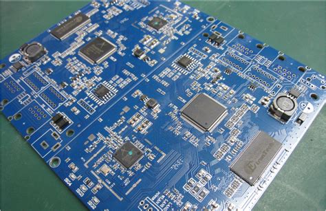
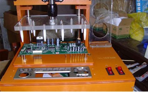
Surface Mount Technology (SMT) forms the backbone of modern PCB assembly, enabling the creation of compact, high-performance electronic systems. In high-density circuit designs, SMT addresses critical challenges such as space constraints, signal integrity, and thermal dissipation by replacing bulkier through-hole components with miniaturized, surface-mounted alternatives. Key to this process is precision component placement, where automated pick-and-place machines position components like micro-BGAs, QFNs, and 01005 resistors with micrometer-level accuracy. This accuracy minimizes parasitic effects and ensures optimal electrical performance in densely packed layouts.
Effective PCBA (Printed Circuit Board Assembly) for high-density applications also demands careful consideration of thermal dynamics. As component densities increase, localized heat buildup can compromise reliability. Advanced substrate materials, such as high-thermal-conductivity laminates and embedded copper cores, help dissipate heat while maintaining structural integrity. Additionally, design for manufacturability (DFM) principles guide layout engineers to balance component spacing, routing complexity, and solder mask requirements, reducing defects during reflow soldering.
Material selection plays a pivotal role in SMT success. Low-temperature co-fired ceramics (LTCC) and polyimide flex substrates enable flexible, multi-layer configurations ideal for wearable devices and IoT applications. Meanwhile, solder paste formulations with fine particle sizes (Type 5 or 6) ensure consistent joint formation for ultra-small components. Rigorous quality control, including 3D solder paste inspection (SPI) and automated optical inspection (AOI), further safeguards against defects like tombstoning or solder bridging.
By integrating these strategies, PCB assembly processes achieve the precision and reliability required for next-generation electronics, from medical implants to 5G infrastructure. The synergy of advanced machinery, innovative materials, and optimized workflows positions SMT as an indispensable enabler of high-density circuit innovation.
Precision Component Placement Techniques for SMT Assembly
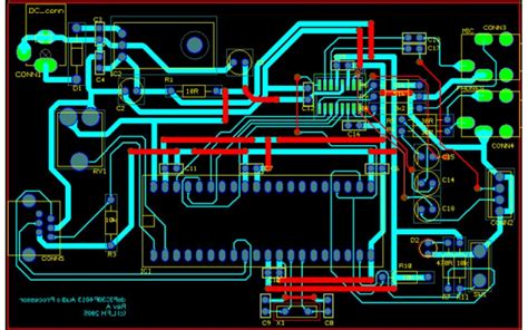
Achieving optimal precision in PCB assembly requires a combination of advanced machinery, meticulous planning, and process refinement. Modern SMT (Surface Mount Technology) workflows rely on automated pick-and-place systems equipped with high-resolution vision systems to ensure accurate alignment of miniature components, such as 0402 or 0201 resistors, on densely packed boards. These systems utilize laser-guided fiducial markers and real-time feedback loops to maintain placement accuracy within ±25 microns, even for ultra-fine-pitch ICs. For PCBA (Printed Circuit Board Assembly) involving high-density designs, stencil optimization plays a critical role—laser-cut apertures with precise tolerances ensure consistent solder paste deposition, minimizing bridging or voids during reflow.
Thermal management is integrated into placement strategies, with components like BGAs (Ball Grid Arrays) positioned to avoid hotspots. Advanced software tools simulate heat distribution and signal integrity pre-assembly, enabling designers to adjust layouts for balanced thermal performance. Additionally, tombstoning and component skew are mitigated through controlled solder paste viscosity and reflow profiles tailored for mixed-component boards.
To enhance reliability in high-density PCB assembly, manufacturers adopt Design for Manufacturability (DFM) principles early in the design phase. This includes standardizing component orientations, maintaining adequate spacing for rework, and selecting materials with compatible thermal expansion coefficients. Automated optical inspection (AOI) and 3D X-ray systems further validate placement accuracy, identifying defects such as misaligned pads or insufficient solder joints before final testing.
As miniaturization trends push the limits of SMT assembly, innovations like vacuum-assisted nozzles for handling ultra-thin components and AI-driven defect detection systems are becoming essential. By integrating these precision techniques, PCBA workflows achieve higher yields and reliability, ensuring robust performance in applications ranging from wearable electronics to aerospace systems.
Advanced Thermal Management Solutions for Compact Circuits
Effective thermal management is critical in PCB assembly for high-density circuit designs, where component miniaturization and increased power density amplify heat dissipation challenges. Advanced thermal solutions must address localized hotspots while maintaining structural integrity and reliability in compact PCBA layouts.
One key strategy involves integrating thermal vias beneath high-power components like BGAs or QFNs. These micro-vias, often filled with conductive epoxy, create vertical pathways to transfer heat from surface-mounted devices to inner copper layers or external heatsinks. For designs requiring ultra-thin profiles, embedded heat spreaders made of aluminum nitride or graphene-enhanced composites offer superior thermal conductivity without compromising space constraints.
| Thermal Interface Material (TIM) | Thermal Conductivity (W/mK) | Application |
|---|---|---|
| Silicone Pads | 3–6 | Low-power ICs |
| Phase Change Alloys | 8–12 | Processors |
| Liquid Metal Compounds | 15–80 | High-density ASICs |
Active cooling methods, such as micro-fans or piezoelectric coolers, complement passive solutions in PCB assembly for mission-critical systems. However, their integration demands precise airflow modeling to avoid interference with adjacent components. Simulation tools like computational fluid dynamics (CFD) enable designers to predict thermal behavior and optimize heatsink geometry or component placement during the PCBA design phase.
Material selection also plays a pivotal role. High-temperature laminates like polyimide or ceramic-filled substrates enhance thermal stability, while selective solder mask removal over copper planes improves heat dissipation. For multi-board systems, thermal interposers with anisotropic conductivity ensure efficient heat transfer between stacked modules without creating electrical short risks.
By balancing material innovation, simulation-driven design, and hybrid cooling architectures, manufacturers can achieve reliable thermal performance in next-generation PCB assembly processes, even as circuit densities continue to escalate.
Optimizing SMT Processes Through Design for Manufacturability (DFM)
Design for Manufacturability (DFM) plays a pivotal role in enhancing the efficiency and reliability of PCB assembly processes, particularly for high-density SMT applications. By integrating DFM principles early in the design phase, engineers can address potential manufacturing challenges, such as component spacing, solder joint integrity, and thermal dissipation, which are critical for PCBA success. A key strategy involves optimizing pad geometries and solder mask designs to accommodate miniaturized components, ensuring precise placement during SMT pick-and-place operations. For instance, reducing pad sizes while maintaining adequate solder volume requires balancing electrical performance with manufacturing tolerances, a task best achieved through collaborative design reviews between engineers and PCB assembly partners.
Thermal management is another critical DFM consideration, especially in densely packed circuits. Implementing thermal relief pads and strategically placing vias can mitigate heat buildup during reflow soldering, preventing warping or delamination. Additionally, selecting materials with compatible coefficients of thermal expansion (CTE) ensures structural stability across temperature cycles, a necessity for high-reliability PCBA applications.
DFM also emphasizes standardization in component libraries to minimize placement errors. Using unified footprints and orientation markings streamlines SMT workflows, reducing rework rates. Automated design validation tools further enhance accuracy by flagging issues like insufficient clearance between components or incompatible solder paste volumes. These tools enable rapid iteration, aligning designs with the capabilities of modern PCB assembly equipment.
Finally, fostering close collaboration between design and manufacturing teams ensures that DFM guidelines are tailored to specific production environments. By addressing yield optimization and process scalability upfront, manufacturers can achieve faster turnaround times and higher-quality outcomes in SMT-driven PCBA projects. This proactive approach not only reduces costs but also positions high-density designs for success in demanding applications.
Quality Control Strategies in High-Density SMT Assembly
Ensuring reliability in high-density PCB assembly demands a multi-layered approach to quality control, particularly when dealing with SMT processes that involve miniature components and tight tolerances. Modern PCBA production lines integrate automated optical inspection (AOI) systems to detect solder joint defects, component misalignment, and bridging in real time. These systems leverage high-resolution cameras and machine learning algorithms to analyze sub-millimeter-scale features, critical for maintaining yield rates in complex designs. For hidden joints, such as those beneath ball grid array (BGA) packages, X-ray inspection (AXI) provides non-destructive testing to identify voids or cracks that could compromise long-term performance.
Thermal profiling plays a pivotal role in SMT assembly quality, as uneven heat distribution during reflow soldering can lead to tombstoning or delamination. Advanced ovens with zone-specific temperature controls and real-time monitoring ensure consistent thermal management across densely populated boards. Additionally, in-circuit testing (ICT) and flying probe testing validate electrical connectivity post-assembly, catching opens or shorts that visual inspections might miss.
Material selection further influences quality outcomes. Using low-voiding solder pastes and high-Tg substrates minimizes risks in high-density PCB applications, where thermal cycling and mechanical stress are amplified. Statistical process control (SPC) tools track production metrics like placement accuracy and solder volume, enabling rapid adjustments to maintain process capability indices (Cp/Cpk) above acceptable thresholds. By combining these strategies, manufacturers achieve robust PCBA reliability even as component densities push the limits of conventional PCB assembly methodologies.
Overcoming Miniaturization Challenges in PCB SMT Production
The relentless push toward miniaturization in modern electronics demands innovative approaches to PCB assembly (PCBA) for high-density designs. As components shrink and circuit complexity increases, manufacturers face challenges in maintaining precision, thermal stability, and reliability. One critical hurdle lies in achieving accurate component placement on densely packed boards. Advanced surface-mount technology (SMT) equipment, such as high-speed pick-and-place machines with vision-guided systems, ensures micron-level alignment even for 01005-sized passives or ultra-fine-pitch ICs. However, tighter spacing amplifies risks like solder bridging, necessitating optimized stencil designs and precise solder paste application.
Thermal management becomes increasingly complex as component density rises. High-power devices in compact layouts generate localized heat, which can degrade performance or shorten lifespan. Integrating thermal vias, heat sinks, or embedded cooling channels within multilayer PCBs helps dissipate heat effectively. Material selection also plays a pivotal role—low-thermal-resistance substrates and high-conductivity solders enhance heat distribution while maintaining electrical integrity.
Design for Manufacturability (DFM) principles are indispensable for overcoming miniaturization challenges. Collaboration between designers and PCBA engineers early in the development phase ensures layouts accommodate manufacturing tolerances, such as pad geometries and solder mask clearances. Leveraging simulation tools to predict thermal and mechanical stresses further reduces prototyping iterations.
Quality control remains paramount, with automated optical inspection (AOI) and X-ray imaging detecting defects like insufficient solder joints or misaligned components. Additionally, material innovations—such as low-temperature co-fired ceramics (LTCC) or high-Tg laminates—improve reliability in high-density environments. By balancing precision SMT processes, advanced materials, and rigorous testing, manufacturers can deliver compact, high-performance solutions tailored to next-generation electronics.
Material Innovations for Reliable High-Density Circuit Performance
Advancements in material science are pivotal to addressing the demands of modern PCB assembly processes, particularly in high-density PCB design. As components shrink and power densities rise, traditional substrates and soldering materials struggle to maintain reliability. Innovations such as low-loss laminates and high-thermal-conductivity substrates are now critical for minimizing signal degradation and managing heat in compact layouts. For instance, ceramic-filled PTFE composites and polyimide-based materials offer exceptional dielectric stability, enabling stable signal transmission even in ultra-thin, multi-layered PCBA designs.
Thermally efficient underfills and advanced solder alloys are also transforming SMT assembly. Materials like silver-doped SAC (tin-silver-copper) solders enhance joint durability while reducing void formation during reflow, a common challenge in densely packed circuits. Additionally, anisotropic conductive films (ACFs) provide precise electrical connections for fine-pitch components, eliminating the risk of bridging in high-density configurations.
Another breakthrough lies in the development of high-reliability conductive adhesives, which replace conventional solders in applications requiring flexibility or resistance to thermal cycling. These adhesives maintain electrical continuity under mechanical stress, making them ideal for wearable electronics or automotive systems. Meanwhile, novel thermal interface materials (TIMs), such as graphene-enhanced gap fillers, dissipate heat more effectively than traditional silicone-based compounds, ensuring sustained performance in power-dense PCBA environments.
By integrating these material innovations, manufacturers can achieve tighter tolerances, improved thermal management, and enhanced longevity in high-density PCB design, all while maintaining compatibility with automated SMT assembly workflows. This synergy between cutting-edge materials and precision manufacturing techniques underscores the evolution of PCB assembly toward meeting the rigorous demands of next-generation electronics.
Future Trends in SMT Assembly for Next-Generation Electronics
The evolution of PCB assembly technologies is poised to address the escalating demands of next-generation electronics, particularly in high-density circuit designs. As devices shrink and performance expectations rise, SMT (Surface Mount Technology) processes are advancing to enable finer pitch components, ultra-compact layouts, and enhanced reliability. A key trend lies in the integration of AI-driven placement systems, which optimize PCBA (Printed Circuit Board Assembly) accuracy by dynamically adjusting for component misalignment and thermal expansion during soldering. These systems leverage machine learning algorithms to predict and mitigate defects, reducing rework and improving yield in complex, multi-layer designs.
Another emerging focus is the adoption of advanced substrate materials such as low-temperature co-fired ceramics (LTCC) and high-frequency laminates, which support higher signal integrity and thermal stability in densely packed circuits. Innovations in PCB assembly workflows now incorporate laser-direct imaging (LDI) and 3D solder paste inspection (SPI) to ensure precise deposition of micro-sized solder joints, critical for miniaturized components like 01005 resistors or wafer-level chip-scale packages (WLCSP). Additionally, the shift toward heterogeneous integration—combining disparate technologies like silicon photonics and embedded passives—is redefining PCBA strategies, enabling seamless coexistence of analog, digital, and RF functionalities on a single board.
Sustainability is also shaping future SMT assembly practices, with manufacturers prioritizing lead-free solders, halogen-free substrates, and energy-efficient reflow ovens to meet global environmental standards. Meanwhile, modular and reconfigurable production lines are gaining traction, allowing rapid adaptation to diverse product lifecycles without compromising throughput. As the industry moves toward 5G, IoT, and AI-driven applications, these advancements in PCB assembly will remain pivotal in balancing miniaturization, performance, and manufacturability for next-generation electronics.
Conclusion
The evolution of PCB assembly methodologies has become pivotal in addressing the complexities of high-density circuit designs. As modern electronics demand greater functionality within shrinking form factors, PCBA processes must balance precision, reliability, and scalability. Key advancements in SMT assembly—such as laser-aligned pick-and-place systems and micro-scale solder paste deposition—enable the accurate placement of ultra-fine-pitch components, ensuring signal integrity even in tightly packed layouts. Equally critical are innovations in thermal management, where advanced heat dissipation materials and embedded cooling structures mitigate thermal stress in compact circuits. By integrating Design for Manufacturability (DFM) principles early in the development cycle, engineers can optimize pad geometries, minimize solder bridging risks, and streamline reflow profiles for consistent PCBA outcomes. Rigorous quality control protocols, including 3D automated optical inspection (AOI) and X-ray testing, further safeguard against defects in high-density assemblies. Emerging material technologies, such as low-loss substrates and high-temperature laminates, enhance electrical performance while supporting the mechanical demands of miniaturized designs. Looking ahead, the convergence of AI-driven process optimization and IoT-enabled production monitoring promises to redefine PCB assembly efficiency, enabling next-generation electronics to meet both performance benchmarks and sustainability goals.
FAQs
What distinguishes high-density PCB assembly from standard SMT processes?
High-density PCB assembly focuses on precise component placement and advanced thermal management to accommodate densely packed circuits. Unlike standard SMT, it employs finer-pitch components, microvias, and specialized materials to ensure reliability in compact designs.
How does Design for Manufacturability (DFM) improve SMT outcomes?
DFM optimizes component layout, pad geometries, and material selection to streamline PCBA workflows. By addressing potential manufacturing challenges early, it reduces defects, enhances yield, and accelerates time-to-market for complex designs.
What thermal management strategies are critical for high-density PCBs?
Effective solutions include thermally conductive substrates, strategic placement of thermal vias, and advanced cooling techniques like embedded heat sinks. These methods mitigate hotspots, ensuring stable performance in space-constrained applications.
Why is automated optical inspection (AOI) vital in quality control?
AOI systems detect solder joint defects, misaligned components, and micro-scale anomalies that manual inspections might miss. This ensures consistency and reliability in high-density PCB assembly, particularly for miniaturized components.
How do material innovations support reliable high-density circuits?
Low-loss dielectrics, high-Tg laminates, and halogen-free substrates improve signal integrity and thermal stability. These materials are essential for maintaining performance in demanding environments like 5G or IoT devices.
What challenges arise from miniaturization in SMT assembly?
Shrinking component sizes increase risks of solder bridging, tombstoning, and thermal stress. Addressing these requires precise stencil design, controlled reflow profiles, and rigorous testing protocols during PCBA production.
What future trends will shape SMT assembly for next-gen electronics?
Emerging trends include ultra-fine-pitch components, 3D-printed circuits, and AI-driven process optimization. These advancements will push the boundaries of high-density PCB design, enabling faster, smaller, and more efficient electronics.
Ready to Optimize Your PCB Assembly Process?
For expert guidance on high-density PCB assembly and tailored PCBA solutions, please click here to explore our services: https://www.andwinpcb.com/pcb-assembly/.


