Summarizing the Design Considerations of PCB Power Supply
When designing a power supply, the importance of a well-layout PCB cannot be overemphasized. In addition, designers must understand the importance of power supply operation to make the job successful.
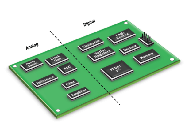
Have you ever wondered how energy is transferred inside the PCB to power our electrical appliances?
There are so many tiny components on a PCB board, and designing such a complex power supply to power each component requires great skill, time, and effort. Moreover, as the density and complexity of circuit design increase, the complexity of the design is also increasing. Only a perfect power supply design can overcome this challenge. However, for a perfect design, all possible problems need to be handled. Some of the issues that need to be addressed include electromagnetic interference, component selection, reducing current loops, and tracking design to handle high currents. In addition, many important parameters such as voltage, current, and heat loss also need to be considered. Let’s take a look at the most important considerations for PCB power supply design.
For power supply design, designers need to perform good PCB layout and plan an effective power distribution network. In addition, designers need to ensure that noisy digital circuit power supplies are separated from critical analog circuit power supplies and circuits. Some important things to consider are discussed below:
1.Choose the right regulator for PCB power supply
Generally, designers have two choices when choosing a power regulator, namely linear regulators and switch mode regulators. Linear regulators provide low noise output but have higher heat dissipation, so a cooling system is required. Switch mode regulators are very efficient over a wide current range, but the switching noise can cause spike responses.
A linear mode requires an input voltage higher than the required output voltage because there will be a minimum voltage drop. A linear regulator will have considerable power loss and heat dissipation, which makes the linear regulator less efficient. If you are considering a linear regulator for your PCB design, you must consider a regulator with a low voltage dropout, and you must perform a thermal analysis before going for manufacturing. Other than that, linear mode regulators are simple, cheap, and provide a noise-free voltage output.
The switching regulator converts one voltage to another by temporarily storing energy in an inductor and then releasing that energy at different switching times. In this power supply, fast switching MOSFETs are used. The output of these highly efficient regulators is adjusted by changing the duty cycle of the pulse width modulation (PWM). The efficiency depends on the heat dissipation of the circuit, which is low in this case.
The PWM switching of the switching regulator causes noise or ripple in the output. The switching current causes noise crosstalk in other signals. Therefore, the switching power supply needs to be isolated from the critical signals.
Switching regulators use MOSFET technology, so it is obvious that these regulators will emit EMI (electromagnetic interference) noise. We cannot completely eliminate EMI from any circuit, but we can minimize it through EMI reduction measures such as filtering, reducing current loops, ground planes, and shielding. Electromagnetic compatibility (EMC) measures should be considered before incorporating a switching mode regulator in your design.
When choosing a regulator, linear and switching regulated power supplies are two obvious choices. Linear controlled power supplies are cheaper, but they are less efficient and dissipate more heat. Meanwhile, switching regulated power supplies are more expensive and require more passive components to be connected, which are not easy to heat up.
2.Thermal management of the power supply
The performance of the power supply directly depends on the heat dissipation. Most electronic components heat up whenever current passes through them. The amount of heat dissipated depends on the power level, characteristics, and impedance of the component. As mentioned earlier, choosing the right regulator can reduce the heat dissipation of the circuit. Switching regulators dissipate less heat and are therefore very efficient.
Electronic circuits operate more efficiently at lower temperatures. To ensure that the device operates at ambient temperature, designers should consider appropriate cooling methods.
If the designer chooses a linear regulator, a heat sink or other cooling method is recommended if the system allows. Fans can be integrated into the design to ensure forced cooling in cases where the device dissipates a lot of heat.
Heat dissipation may not be uniform across the PCB. Components with high power ratings may dissipate a lot of heat, creating hot spots around them. Thermal vias can be used near these components to quickly transfer heat away from the area.
A combination of heat dissipation techniques and cooling methods can create an efficient power supply design. Designers can use conduction cooling methods such as heat sinks, heat pipes, thermal vias, or convection cooling methods such as cooling fans, thermoelectric coolers, etc.
3.Ground and power planes to improve PCB power supply
Summarize the design considerations of PCB power supply
The ground plane and power plane are low impedance paths for power transmission. Power supplies require separate ground planes to distribute power, reduce EMI, minimize crosstalk, and reduce voltage drop. The power plane is dedicated to transferring power to the required areas of the PCB.
PCB designers need to treat each part of the ground network separately. In a multi-layer PCB, one or more layers can be dedicated to ground and power planes. Moreover, they can effectively connect the signal traces to the ground by placing a ground plane between two active signal layers to reduce interference and crosstalk.
4.Decoupling capacitors and bypass capacitors
Summarize the design considerations of PCB power supply
When distributing power to components on the full board, different active components will cause ground bounce and ringing in the power rails. This can cause voltage drops near the power pins of the components. In this case, designers use decoupling and bypass capacitors near the power pins of the components to make short spikes in the current demand of the device.
The concept behind decoupling is to reduce the impedance between the power supply and the ground.
Decoupling capacitors act as secondary power supplies to provide the current required by the IC. and act as a local charge source to support switching events.
Bypass capacitors bypass noise and reduce fluctuations in the power bus. They are placed close to the device or IC and linked between the power supply and ground to compensate for changes in the power and ground plane potential when many ICs switch simultaneously.
Bypass capacitors are used to suppress inter-system or intra-system noise within the power grid. All decoupling capacitors must be connected close to the power pins of the IC and the other end directly to the low impedance ground plane. Short traces to the decoupling capacitors and ground vias are required to minimize the series inductance of this connection.
When selecting local bypass capacitors, several aspects need to be considered. These factors include choosing the correct capacitor value, dielectric material, geometry, and location of the capacitor relative to the IC. A typical value for a decoupling capacitor is 0.1μF ceramic.
5.EMI Filtering EMI radiation can come from any power line entering and exiting the power supply housing.
PCB designers expect the power supply to keep its EMI below its defined spectrum limits. Therefore, EMI filters are used at the power input point to reduce conducted noise.
The architecture of the EMI filter allows it to block high-frequency noise. It is critical that designers carefully lay out filter circuit components to prevent components from transferring energy into the traces that connect them.
6.Frequency Response of Power Transmission Systems When a power supply is suddenly loaded, such as from no load to full load, the voltage output will tend to drop briefly and return to normal voltage. In some cases, the output will oscillate for a period of time before the voltage stabilizes to normal levels. If the oscillation is beyond the design limit, it is necessary to adjust the output capacitor and compensation capacitor. For example, for the LM7805, it is recommended to place a 0.1μF capacitor next to the output pin. Similarly, sudden unloading of the regulator may cause overshoot and oscillation.
To get better response from the circuit design, ensure that the selected components are within the design constraints. Whether the circuit is AC or DC, they respond differently. AC and DC circuits should be considered separately.
- Power Integrity (PI) Designers should ensure the power integrity of the power supply design. Power integrity is simply the quality of the power delivered to the circuit. It is a measure of the efficiency of the transfer of power from the system to the load within the system, and it ensures that all circuits and devices are provided with appropriate power, thereby achieving the desired circuit performance.
A power supply with less noise ensures higher power integrity. Power integrity design is nothing but managing power supply noise. There are simulation tools that help estimate the power quality of a circuit. Such tools help estimate voltage drops, suggest decoupling capacitors, and also identify hot spots in a circuit with high currents.
Conclusion A good power supply is key to accurate functioning of electronic devices. As we have seen, PCB designers have several options to choose from when considering power supply design. It is important to select regulators, capacitors, and EMI filtering considering these factors. Similarly, thermal effects and load response should also be considered while designing a power system.
At the same time, follow the recommendations mentioned in the power IC datasheet. The thickness of traces and placement of components play a vital role in power supply design.


