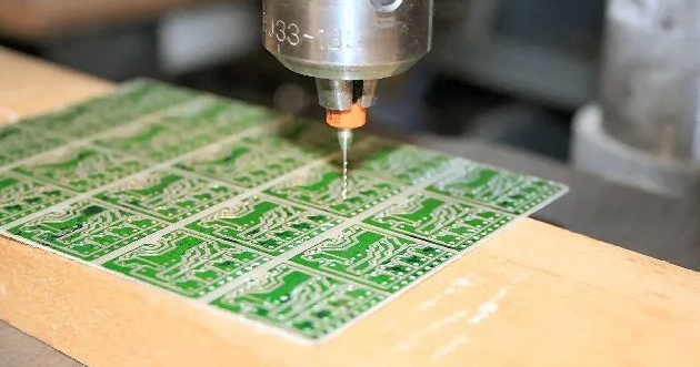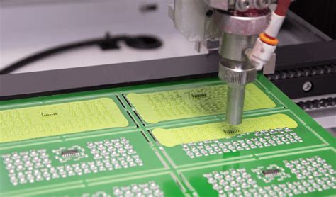
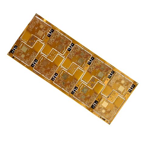
Ten problems about PCB defects
1.[Delamination]
Delamination is a long-standing problem of PCB, and ranks first among common problems. The reasons for its occurrence may be as follows:
(1) Improper packaging or storage, dampness;
(2) Storage time is too long, exceeding the shelf life, PCB board dampness;
(3) Supplier material or process problems;
(4) Poor design material selection and copper surface distribution.
The dampness problem is relatively easy to occur. Even if you choose a good packaging and there is a constant temperature and humidity warehouse in the factory, the transportation and temporary storage process cannot be controlled. The author once had the “fortune” to visit a bonded warehouse. Don’t count on temperature and humidity management. The roof is still leaking and the boxes are directly in the water. However, dampness can still be dealt with. Vacuum conductive bags or aluminum foil bags can well protect against water vapor intrusion. At the same time, a humidity indicator card is required in the packaging bag. If the humidity card is found to be over the standard before use, baking before going online can generally solve the problem. The baking conditions are usually 120 degrees and 4 hours.
If there is a problem with the materials or processes of the mobile phones and other products provided by the supplier at the mobile phone exhibition, the possibility of scrapping is relatively high.
Common possible reasons include: poor browning (blackening), PP or inner layer board dampness, insufficient PP glue, abnormal lamination, etc. In order to reduce the occurrence of such problems, special attention should be paid to the management of the corresponding process by the PCB supplier and the reliability test of stratification. Taking the thermal stress test in the reliability test as an example, the standard requirement of a good factory is that there should be no stratification for more than 5 times, which will be confirmed in the sample stage and each cycle of mass production, while the standard of ordinary factories may only be passed twice, and it will be confirmed once every few months. The IR test of simulated mounting can also prevent the outflow of defective products more, which is a must for excellent PCB factories.
Of course, the PCB design of the design company itself will also bring hidden dangers of stratification. For example, the selection of Tg of the board is often not required. In order to save costs, the PCB factory will definitely choose ordinary Tg materials, and the temperature resistance will be relatively poor. In the era when lead-free has become the mainstream, it is safer to choose Tg above 145°C. In addition, large empty copper surfaces and overly dense buried hole areas are also hidden dangers of PCB delamination, which need to be avoided during design.

2.[Poor solderability]
Solderability is also one of the more serious problems, especially batch problems. The possible causes are board surface pollution, oxidation, black nickel, abnormal nickel thickness, solder mask SCUM (shadow), long storage time, moisture absorption, solder mask on PAD, too thick (repair).
Pollution and moisture absorption problems are relatively easy to solve, while other problems are more troublesome, and there is no way to find them through incoming material inspection
At this time, it is necessary to pay attention to the process capabilities and quality control plans of the PCB factory. For example, for black nickel, it is necessary to see whether the PCB factory outsources the chemical gold, whether the frequency of analyzing its own chemical gold wire solution is sufficient, whether the concentration is stable, whether regular gold stripping tests and phosphorus content tests are set up for detection, and whether the internal solderability test is well executed. If all can be done well, the possibility of batch problems is very small. As for poor PAD and repair on solder mask, it is necessary to understand the standards set by PCB suppliers for inspection and maintenance, whether inspectors and maintenance personnel have a good assessment and employment system, and clearly define that dense pad areas cannot be repaired (such as BGA and QFP).
3.[Board bending and warping]
The reasons that may cause board bending and warping include: supplier material selection problems, abnormal production process, poor rework control, improper transportation or storage, insufficient design of broken holes, and large differences in copper area of each layer. The last two design problems need to be avoided through design review in the early stage. At the same time, the PCB factory can be required to simulate the IR conditions of mounting to test to avoid the bad board bending after the furnace. For some thin boards, it can be required to pack the wood pulp board up and down before packaging to avoid subsequent deformation. At the same time, a clamp is added during mounting to prevent the device from bending the board due to excessive weight.
4.[Scratches and exposed copper]
Scratches and exposed copper are the most challenging defects in the management system and execution of PCB factories. This problem is not serious, but it does bring quality concerns. Many PCB companies will say that this problem is difficult to improve. The author has promoted the improvement of scratches in many PCB factories and found that many times it is not that the improvement is not good, but whether to improve it or not, and whether there is motivation to improve it. All PCB factories that seriously promote the project have significantly improved the DPPM delivered. So the trick to solve this problem is: push and press.
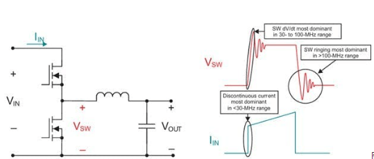
5.[Poor impedance]
The impedance of PCB is an important indicator related to the RF performance of mobile phone boards. The common problem is that the impedance difference between PCB batches is relatively large. Since the impedance test strip is generally made on the large board edge of the PCB and will not be shipped with the board, the supplier can be asked to attach the impedance strip and test report of the batch for reference each time it ships, and also require the comparison data of the board edge wire diameter and the board inner wire diameter
6.[BGA solder void]
BGA solder voids may cause poor function of the main chip, and may not be found in the test, and the hidden risk is very high. Therefore, many patch factories now will conduct X-RAY inspection after mounting. The possible reasons for this kind of defect are residual liquid or impurities in the PCB hole, which vaporizes after high temperature, or the laser hole shape on the BGA pad is poor. Therefore, many HDI boards now require electroplating to fill holes or semi-fill holes to avoid this problem.
7.[Solder mask blistering/falling off]
This kind of problem is usually caused by abnormal control of the PCB solder mask process, or the selection of inappropriate solder mask ink (cheap, non-metallic gold ink, not suitable for mounting flux), or the temperature of the patch or rework is too high. To prevent batch problems, PCB suppliers need to formulate corresponding reliability test requirements and control them at different stages.
8.[Poor plugging]
Poor plugging is mainly caused by insufficient technical capabilities of PCB factories or simplified processes. It is manifested as incomplete plugging, copper exposure or false copper exposure in the hole ring. It may cause insufficient solder, short circuit with patch or assembled device, residual impurities in the hole, etc. This problem can be found in the appearance inspection, so it can be controlled in the incoming material inspection, and the PCB factory is required to improve it.
9.[Poor size]
There are many possible reasons for poor size. The PCB production process is prone to expansion and contraction. The supplier adjusts the drilling program/graphic ratio/molding CNC program, which may cause problems such as easy displacement of the mounting and poor matching of structural parts. Since such problems are difficult to detect, they can only rely on the supplier’s good process control, so special attention needs to be paid when selecting suppliers.
10.[Galvani effect]
The Galvani effect is the galvanic cell reaction learned in high school chemistry, which appears in the OSP process of selective gold-plated boards. Due to the potential difference between gold and copper, the copper pads connected to the large gold surface will continue to lose electrons and dissolve into divalent copper ions during the OSP process, causing the pads to become smaller, affecting the subsequent component mounting and reliability.
Although this problem does not occur often and has never appeared in Plato, once it occurs, it is a batch problem. Board manufacturers with experience in mobile phone PCB production will screen out this part of the pads through computer software, pre-compensate during design, and set special rework conditions and limit the number of reworks in the OSP process to avoid problems. Therefore, this problem can be confirmed in advance when auditing the board factory.