The Application of DFM Inspection in PCB Design Software CAM350
Abstract
Design for Manufacturability (DFM) is a critical aspect of printed circuit board (PCB) design that ensures the design can be efficiently and reliably manufactured. CAM350, a widely used PCB design analysis and verification tool, plays a significant role in performing DFM checks to identify potential manufacturing issues before production. This paper explores the application of DFM inspection in CAM350, discussing its key features, benefits, and impact on PCB manufacturing efficiency.
1. Introduction
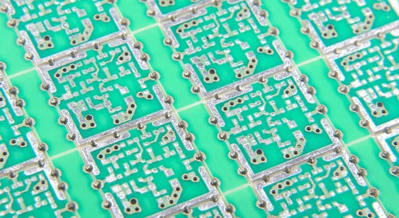
The complexity of modern PCB designs has increased significantly, with higher layer counts, finer trace widths, and advanced manufacturing techniques. Ensuring that a PCB design is manufacturable requires thorough DFM analysis to detect errors that could lead to production failures, increased costs, or delays.
CAM350, developed by DownStream Technologies, is a powerful software tool used for PCB fabrication and assembly analysis. It provides comprehensive DFM checks to validate designs against manufacturing constraints, helping engineers optimize their layouts for production.
2. Understanding DFM in PCB Design
DFM (Design for Manufacturability) is a methodology aimed at designing PCBs in a way that minimizes production difficulties while maintaining performance and reliability. Key aspects of DFM include:
- Manufacturing Constraints Compliance – Ensuring the design adheres to fabrication capabilities (e.g., minimum trace width, hole size, spacing).
- Assembly Feasibility – Verifying component placement, soldering, and thermal management.
- Cost Optimization – Reducing unnecessary complexities that increase production costs.
- Yield Improvement – Minimizing defects and rework by detecting potential issues early.
3. CAM350’s Role in DFM Inspection
CAM350 integrates advanced DFM analysis tools that allow designers to validate their PCB layouts before sending them to fabrication. The software performs automated checks based on predefined manufacturing rules, ensuring compliance with industry standards.
3.1 Key DFM Checks in CAM350
CAM350 provides a wide range of DFM verification features, including:
A. Fabrication-Related DFM Checks
- Minimum Trace Width and Spacing
- Ensures traces meet the manufacturer’s minimum width and spacing requirements.
- Prevents etching issues and short circuits.
- Drill-to-Copper Clearance
- Verifies adequate spacing between drilled holes and nearby copper features.
- Avoids drill breakout or electrical shorts.
- Annular Ring Integrity
- Checks if pads have sufficient copper around drilled holes for reliable plating.
- Ensures proper via and through-hole connections.
- Copper Slivers and Acid Traps
- Detects thin copper slivers that may break during etching.
- Identifies acute angles that could trap chemicals, leading to uneven etching.
- Solder Mask and Silkscreen Clearance
- Validates solder mask openings and silkscreen alignment.
- Prevents mask bridging or misprinted component labels.
B. Assembly-Related DFM Checks
- Component Placement Analysis
- Ensures adequate spacing between components for soldering.
- Detects potential tombstoning or solder bridging risks.
- Solder Paste Coverage
- Verifies stencil design for proper solder paste application.
- Optimizes pad-to-paste ratio for reliable solder joints.
- Thermal Relief Verification
- Checks thermal relief connections on ground and power planes.
- Ensures proper heat dissipation during soldering.
3.2 Automated DFM Rule Checking
CAM350 allows users to define custom DFM rules based on specific manufacturer capabilities. The software can automatically scan the design and flag violations, such as:
- Insufficient pad sizes for component leads.
- Missing or misaligned fiducials for assembly alignment.
- Incorrect layer stackup affecting impedance control.
4. Benefits of Using CAM350 for DFM Inspection
4.1 Early Detection of Design Flaws
By performing DFM checks in CAM350, engineers can identify and resolve issues before fabrication, reducing costly re-spins and delays.
4.2 Improved Manufacturing Yield
DFM validation ensures that the PCB design aligns with production capabilities, minimizing defects and improving yield rates.
4.3 Cost Savings
Detecting and correcting errors early reduces scrap, rework, and production delays, leading to significant cost savings.
4.4 Enhanced Collaboration Between Design and Manufacturing Teams
CAM350’s reporting tools allow designers to share DFM findings with manufacturers, ensuring alignment on design constraints.
5. Case Study: DFM Analysis in CAM350
A case study involving a high-density PCB design demonstrated how CAM350’s DFM checks prevented manufacturing failures:
- Issue: A 6-layer PCB had insufficient annular rings on several vias.
- CAM350 Detection: The software flagged the violation during DFM analysis.
- Resolution: The designer adjusted the via pad sizes before fabrication, avoiding potential open circuits.
6. Conclusion
DFM inspection in CAM350 is a crucial step in PCB design validation, ensuring manufacturability, reliability, and cost-efficiency. By leveraging CAM350’s automated DFM checks, engineers can detect and resolve potential issues early, improving production success rates. As PCB designs continue to evolve, integrating robust DFM tools like CAM350 will remain essential for achieving high-quality, manufacturable designs.