The Art of Perfect PCB Assembly: Mastering the Core Components for Flawless Results
Key Takeaways
PCB assembly requires a careful and meticulous approach to achieve flawless results.
Select the right components for your PCB assembly projects to ensure optimal performance.
Understand the importance of PCB layout and how it impacts the overall functionality of your electronic circuits.
Efficient component placement techniques play a crucial role in ensuring proper functionality and reliability in PCB assembly.
Mastering soldering methods is essential for creating robust and durable connections between components.
Troubleshoot common issues in PCB assembly to overcome challenges and ensure a successful outcome.
Follow best practices for flawless results, including thorough testing, quality control, and adherence to industry standards.
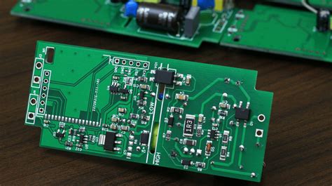
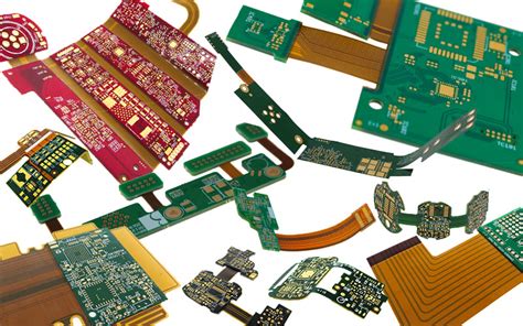
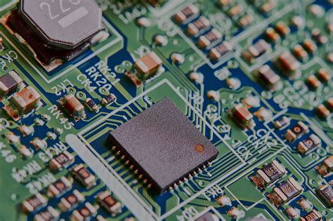
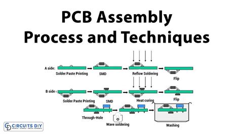
PCB assembly, also known as PCBA, encompasses a range of processes involved in creating electronic circuits. It is a delicate art that requires precision and attention to detail. To achieve flawless results in your PCB assembly projects, you need to master the core components involved. This comprehensive guide will equip you with the knowledge and skills necessary to excel in every aspect of PCB assembly.
Selecting the right components is a critical first step in the PCB assembly process. The quality and compatibility of the chosen components directly impact the performance and reliability of your electronic circuits. By understanding component specifications, such as voltage ratings, current limitations, package types, and environmental tolerances, you can ensure optimal functionality.
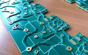
Another crucial aspect of successful PCB assembly is understanding PCB layout. The arrangement of components on a circuit board affects signal integrity, electromagnetic compatibility (EMC), thermal management, and ease of manufacturing. By considering factors like trace lengths, component spacing, ground planes, and signal routing techniques, you can optimize circuit performance.
Efficient component placement techniques are essential for maintaining signal integrity and minimizing potential issues like crosstalk or electromagnetic interference (EMI). Properly positioning components according to their functionality and thermal requirements improves reliability and ease of manufacturing. Careful consideration should also be given to connector placement for convenient access during assembly and maintenance.
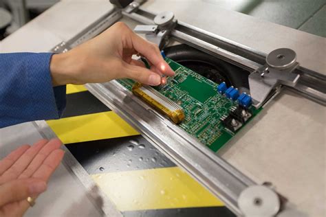
Mastering soldering methods is an indispensable skill for flawless PCB assembly. The quality of solder joints directly affects the longevity and performance of the circuit board. Understanding soldering techniques, such as reflow soldering or hand-soldering, as well as proper temperature profiles, flux application, and inspection methods, will ensure reliable connections.
Even with careful planning and execution, it’s important to be prepared to troubleshoot common issues that may arise during PCB assembly. Problems like inadequate solder joints, short circuits, or component failures can occur despite thorough preparation. By having a solid understanding of troubleshooting techniques and utilizing appropriate tools, you can address these challenges effectively.
To consistently achieve flawless results in PCB assembly, it is crucial to adhere to best practices. Thoroughly test your assembled PCBs for functionality and conduct quality control checks to ensure compliance with industry standards. Maintain meticulous documentation of your manufacturing processes and employ rigorous inspection procedures throughout the production cycle.
In conclusion, mastering the art of PCB assembly requires in-depth knowledge of core components and meticulous attention to detail. By selecting the right components, understanding PCB layout intricacies, employing efficient component placement techniques, mastering soldering methods, troubleshooting common issues effectively, and following best practices throughout the process, you can create flawless electronic circuits with confidence and finesse.
Remember: pcb assembly is an art form that demands patience, precision, and a passion for excellence. With dedication and practice, you can unlock the secrets to mastering this intricate craft.
Efficient Component Placement Techniques
Efficient component placement is a crucial aspect of achieving flawless results in PCB assembly. The way components are arranged on the PCB can greatly impact the overall performance and reliability of the electronic circuit. Here, we will explore some key techniques to help you master the art of efficient component placement.
1. Careful Consideration of Component Orientation
When placing components on a PCB, it is important to consider their orientation. Proper alignment ensures optimal electrical connections and simplifies the assembly process. Make sure that polarized components, such as electrolytic capacitors and diodes, are correctly positioned to align with the circuit diagram.
2. Grouping Components by Functionality
Organizing components based on their functionality can enhance the overall layout and ease troubleshooting in case any issues arise. Grouping components that work together logically will minimize signal interference and improve signal integrity. It also simplifies testing and maintenance processes.
3. Minimizing Trace Lengths
Reducing trace lengths between components is a critical technique for improving signal integrity and reducing electrical noise. Shorter traces lead to better performance, as they minimize the effects of parasitic capacitance and inductance. By planning the placements strategically, you can achieve compact designs with optimized trace lengths.
4. Thermal Considerations
Certain components generate heat during operation, such as power transistors or voltage regulators. It is vital to consider thermal management when placing these components on the PCB to ensure optimal performance and reliability. Adequate spacing between heat-generating components and other sensitive parts prevents thermal interference and potential damage.
5. Compliance with Design for Manufacturing (DFM) Guidelines
To ensure smooth manufacturing processes and efficient assembly, it is crucial to follow Design for Manufacturing (DFM) guidelines provided by your PCB manufacturer or industry standards. These guidelines cover aspects like component spacing, solder mask clearance, and proper pad sizes for surface mount components. Adhering to DFM guidelines minimizes manufacturing errors and improves overall PCB quality.
6. Use of PCB Design Software Tools
Utilizing advanced PCB design software tools can significantly streamline the component placement process. These tools offer features like automatic component placement, design rule checks, and 3D visualization, enabling precise component arrangement and identification of potential issues beforehand.
By employing efficient component placement techniques, you can optimize the performance, reliability, and manufacturability of your PCB assemblies. Paying attention to component orientation, grouping components by functionality, minimizing trace lengths, considering thermal aspects, following DFM guidelines, and leveraging PCB design software tools will set you on the path towards flawless results in your PCB assembly projects.
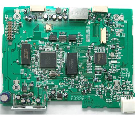
Introduction to PCB Assembly
PCB assembly, also known as PCBA, is a crucial process in the manufacturing of electronic devices. It involves combining various electronic components onto a printed circuit board (PCB) to create functional electronic circuits. This process requires precision, attention to detail, and a deep understanding of the core components involved.
When it comes to PCB assembly, flawless execution is essential for ensuring the functionality and reliability of electronic devices. Achieving optimal results requires a systematic approach and adherence to best practices throughout the assembly process. In this article, we will explore the intricacies of PCB assembly and provide valuable insights to help you master this art.
Selecting the Right Components
In the world of PCB assembly, selecting the right components is crucial for achieving flawless results. Whether you’re a seasoned professional or a novice in the field, understanding how to choose the right components will set the foundation for success in your projects. So let’s dive into some key considerations when it comes to reaching impeccable outcomes in PCB assembly.
“The key to flawless PCB assembly lies in selecting the right components.” – Anonymous
Quality is Paramount
When it comes to choosing components for your PCB assembly, quality should be your top priority. Opt for reputable brands and suppliers that offer reliable and well-tested components. Investing in high-quality parts may seem like an added expense, but it pays off in the long run by ensuring optimal performance and longevity of your electronic circuits.
Compatibility and Specifications
Another crucial aspect to consider is component compatibility. Ensure that each component you select is compatible with your design requirements and fits seamlessly with other parts on the board. Pay attention to specifications such as voltage ratings, current ratings, temperature ranges, and physical dimensions. Matching these specifications will help avoid any compatibility issues down the line.
Consider Assembly Techniques
When choosing components for PCB assembly, it’s essential to consider the assembly techniques you’ll be using. Take into account whether you’ll be hand soldering or using automated pick-and-place machines. Some components may be better suited for specific assembly methods due to their size, package type, or sensitivity to heat. Adapting your component selection to align with your chosen assembly techniques will greatly contribute to flawless results.
Environmental Factors
The environment in which your electronic circuits will operate should also influence your component selection process. Consider factors such as temperature extremes, humidity levels, and exposure to vibration or shock. Choosing components that are specifically designed for harsh environments will ensure reliability and durability under challenging conditions.
“To achieve harmony between form and function in PCB assembly, consider the environmental factors that your circuits will face.” – Anonymous
Keep these tips in mind when selecting components for your PCB assembly projects, and you’ll be on your way to achieving flawless results. Remember, it’s all about finding the right balance between high-quality components, compatibility with your design, suitable assembly techniques, and consideration of environmental factors. With the right choices, your electronic circuits will perform with confidence and finesse!
Keep reading as we delve deeper into the art of perfect PCB assembly. In our next section, we’ll explore the intricacies of understanding PCB layout.
Stay tuned for more insights and expert advice on mastering the core components for flawless results in PCB assembly!
*Note: PCB Assembly includes PCB and PCBA
Understanding PCB Layout
In the realm of PCB assembly, achieving flawless results greatly relies on understanding the intricacies of PCB layout. Proper layout plays a fundamental role in ensuring optimal functionality and performance of electronic circuits. By mastering the art of PCB layout, you can elevate your assembly projects to new heights of excellence.
Importance of PCB Layout
The layout of a printed circuit board (PCB) involves arranging components and connecting them with traces to form a functional circuit. A well-designed layout minimizes signal interference, reduces noise, and enhances overall reliability. Each component must be strategically placed to ensure efficient signal flow and avoid potential issues such as crosstalk or electromagnetic interference.
Considerations for Effective Layout
When diving into PCB layout, several key considerations come into play. Firstly, understanding the electrical characteristics of components is vital. Each component requires proper spacing considerations to prevent electrical interference or short circuits.
Secondly, paying attention to the size and shape of traces is crucial. Wider traces can carry more current without overheating, while thinner traces are suitable for low-current signals. Proper trace spacing must also be maintained to prevent signal coupling.
Thirdly, efficient component placement involves strategic positioning based on functionality and thermal considerations. Component proximity should be optimized to minimize signal path lengths and reduce parasitic capacitance or inductance effects.
Designing for Manufacturability
While focusing on PCB layout, it is important to keep manufacturability in mind. Designing boards that can be easily manufactured saves time, cost, and effort during assembly processes.
To ensure manufacturability, consider the capabilities and limitations of the manufacturer’s equipment and processes. Proper spacing between components should allow for efficient soldering techniques without risking shorts or open connections. Moreover, designing with standard component packages readily available in the market streamlines the procurement process.
Industry Standards and Tools
In the world of PCB layout, adhering to industry standards is essential. Familiarize yourself with guidelines for trace widths, clearance, and spacing provided by organizations such as the Institute of Electrical and Electronics Engineers (IEEE). Additionally, utilize reliable layout design software that offers advanced features such as auto-routing, design rule checks, and 3D visualization.
Conclusion
Mastering PCB layout is a fundamental skill for achieving flawless results in PCB assembly. By understanding the importance of layout considerations, designing for manufacturability, and adhering to industry standards, you can elevate your circuit designs to new levels of excellence. With each project, continue to refine your skills and embrace the art of PCB assembly with confidence and finesse.
Note: This article is focused on understanding PCB layout. For information about selecting the right components or mastering soldering methods, please refer to the respective sections in this comprehensive guide.
Efficient Component Placement Techniques
Efficient component placement is a critical aspect of successful PCB assembly. By strategically positioning the core components on the PCB, you can optimize performance, minimize signal interference, and enhance overall reliability. Here, we will explore some key techniques to help you master the art of efficient component placement.
1. Grouping Components by Functionality
One effective technique is to group components based on their functionality. By doing so, you can minimize signal paths and reduce the chances for electromagnetic interference (EMI). For example, if you have a section of the circuit dedicated to power regulation, consider placing all related components close together. This not only improves signal integrity but also facilitates easier troubleshooting and maintenance in the future.
2. Considering Signal Flow
Another crucial factor to consider is the direction of signal flow within your PCB layout. Arrange components in a way that follows the natural flow of signals through your circuit. This approach helps to reduce crosstalk and ensures smooth transmission paths. By carefully organizing components according to signal flow, you can minimize both electrical noise and potential timing issues.
3. Thermal Management
Efficient component placement also involves considering thermal management. Certain components generate heat during operation, and it’s important to position them strategically to avoid hotspots and thermal dissipation issues. Distributing heat-generating elements evenly across the board can prevent overheating and ensure optimal performance.
4. Utilizing Reference Designs
Reference designs provided by component manufacturers can be invaluable resources for efficient component placement. These designs offer insights into recommended footprints, layouts, and optimal placements for specific components. By leveraging these references, you can save time while maximizing performance and reliability.
5. Using PCB Design Software Tools
PCB design software tools provide advanced features that can significantly aid in efficient component placement. These tools offer functionalities such as automated placement algorithms that optimize proximity and eliminate manual errors. Leveraging such tools can help you achieve the best possible component placement results, even for complex designs.
In summary, efficient component placement techniques play a vital role in ensuring flawless results in PCB assembly. By grouping components by functionality, considering signal flow, managing heat dissipation, utilizing reference designs, and leveraging PCB design software tools, you can optimize performance and enhance the reliability of your electronic circuits. Implement these techniques in your PCB assembly projects to achieve impeccable results and take your electronics skills to new heights.
Mastering Soldering Methods
In the realm of PCB assembly, mastering soldering methods is essential for achieving flawless results. This crucial skill involves the art of securely and accurately connecting electronic components to the printed circuit board (PCB). Whether you’re a novice or an experienced engineer, honing your soldering techniques will enable you to create impeccable electronic circuits with confidence and finesse.
The Importance of Proper Soldering
Effective soldering ensures the reliable and durable performance of your PCB assembly. This process involves melting a solder alloy, which is typically composed of tin and lead, to create a strong bond between the component leads and the PCB pads. When done correctly, soldering provides excellent electrical conductivity and mechanical stability.
Key Techniques for Successful Soldering
Preparation: Before diving into the soldering process, it’s crucial to prepare your work area properly. Ensure that you have a clean, well-ventilated space with ample lighting. Gather all the necessary tools, such as a soldering iron with an appropriate tip size, solder wire, flux, and a desoldering pump or braid for potential rework.
Component Placement: Accurate component placement is fundamental for successful soldering. Align each component precisely with its designated location on the PCB. Take care to avoid contaminating sensitive parts during handling.
Temperature Control: Controlling the temperature of your soldering iron is vital to prevent damage to both components and PCBs. Adjust it according to the specific requirements of your project. Generally, a temperature between 300°C and 350°C (572°F – 662°F) is sufficient for most applications.
Applying Flux: Flux facilitates proper wetting between the component leads and pads, ensuring a reliable connection. Apply an appropriate amount of flux before soldering each joint but avoid excessive use as it may cause flux residue buildup.
Soldering Techniques: There are various soldering techniques, but two common methods are through-hole soldering and surface mount soldering. Through-hole soldering involves heating the joint from the opposite side of the component lead, allowing the solder to flow and form a solid connection. Surface mount soldering, on the other hand, utilizes smaller components with metal contacts that adhere directly to the PCB surface.
Joint Inspection: After soldering a joint, inspect it visually to ensure a smooth and shiny appearance with no bridging or cold solder joints. Additionally, check for proper alignment to verify that components are flush with the PCB.
Continuous Learning for Excellence
Mastering soldering methods is an ongoing journey of improvement and refinement. Stay updated with emerging technologies and industry advancements in PCB assembly. By continuously enhancing your knowledge and skills, you can tackle increasingly complex projects with confidence.
In conclusion, proficiency in soldering is an invaluable asset when it comes to achieving flawless PCB assembly results. With proper preparation, precise component placement, controlled temperature, flux application, appropriate soldering techniques, and diligent joint inspection—you’ll be well on your way to creating impeccable electronic circuits. Embrace the artistry of soldering and unlock endless possibilities in your PCB assembly endeavors!
Troubleshooting Common Issues in PCB Assembly
PCB assembly is a meticulous process that requires attention to detail and precision. Despite taking utmost care, issues can arise during the assembly phase. In this section, we will explore some common problems that may occur and discuss effective troubleshooting techniques to overcome them.
Insufficient Solder Joints
One of the most common issues faced in PCB assembly is the presence of insufficient or weak solder joints. These joints are critical for establishing electrical connections and ensuring the overall integrity of the circuit. Insufficient solder can result in intermittent or non-functional connections, leading to poor performance or complete malfunctioning of the PCB.
To troubleshoot this issue, it is crucial to inspect each solder joint carefully. Look for joints with thin or incomplete solder coverage. If identified, reflow the solder by applying heat using a soldering iron or a reflow station. Ensure that proper flux is used to maintain good wetting and adhesion between components and pads.
Solder Bridges
Solder bridges occur when excess solder flows between adjacent pads or pins, causing an unintended connection. These bridges can short circuit components and disrupt the functionality of the PCB.
To address this problem, visually inspect each joint for any signs of adjacent connections. Employ a magnifying glass if necessary for better accuracy. Gently remove excess solder using desoldering wick or a vacuum suction tool. Be cautious during this process to avoid damaging nearby components.
Component Misalignment
Improper component placement can lead to issues such as incorrect functioning or complete failure of the PCB. Components must be accurately aligned with their respective footprints on the board during assembly.
If you suspect misalignment of components, carefully examine their positions relative to their footprints using visual inspection aids like magnifying glasses or microscopes. In case of misalignment, use tweezers or a vacuum suction tool to lift and reposition the component correctly.
Component Damage
During the handling or assembly process, delicate components can be susceptible to damage, impairing their functionality. Damage can include bent pins, cracked leads, or even surface contamination.
To troubleshoot this issue, scrutinize each component for visible signs of damage. If damage is detected, carefully replace the damaged component with a new one while adhering to proper ESD precautions.
By employing these troubleshooting techniques, you can rectify common issues that may arise during PCB assembly. Remember to exercise patience and precision while identifying and addressing these problems. With practice and experience, you will become adept at troubleshooting and ensure flawless results in your PCB assembly projects.
Best Practices for Flawless Results in PCB Assembly
When it comes to achieving flawless results in PCB assembly, following best practices is essential. Whether you are a seasoned professional or just starting out, implementing these techniques will help you excel in your electronic projects. Here, we bring you some key tips and guidelines to ensure impeccable PCB assembly:
1. Selecting the Right Components
The foundation of a successful PCB assembly lies in choosing the right components. Take into account factors such as reliability, performance, and compatibility with your design specifications. Thoroughly research and evaluate different options before making your final selection. By using high-quality components, you eliminate the risk of failure due to poor quality materials.
2. Understanding PCB Layout
A well-designed PCB layout is crucial for ensuring optimal performance. Familiarize yourself with industry standards and guidelines for component placement, trace routing, and signal integrity. Consider factors like noise reduction and thermal management during the layout process. Adopting a systematic approach and using specialized layout software can greatly enhance the efficiency and accuracy of your design.
3. Efficient Component Placement Techniques
Proper component placement plays a critical role in achieving reliable PCB assembly. Take advantage of automated placement tools to ensure precise positioning of components on the board. Pay attention to factors such as signal integrity, thermal considerations, and ease of soldering. Optimize component placement to minimize signal delays and reduce the chances of cross-talk between traces.
4. Mastering Soldering Methods
Soldering is a skill that requires practice and attention to detail. Ensure that you use appropriate soldering techniques to establish reliable electrical connections between components and the PCB. Familiarize yourself with different soldering methods such as through-hole soldering and surface mount technology (SMT). Use high-quality soldering equipment and follow industry standards for temperature profiles, flux application, and solder joint inspection.
5. Troubleshooting Common Issues in PCB Assembly
Even with careful planning and execution, issues can arise during PCB assembly. Develop troubleshooting skills to identify and rectify common problems such as solder bridging, cold solder joints, or component misalignment. Utilize diagnostic tools like multimeters and oscilloscopes to test and verify the functionality of your assembled PCBs. Address any issues promptly to ensure the reliability of your circuits.
By implementing these best practices, you can significantly improve the quality and reliability of your PCB assembly projects. The art of flawless PCB assembly lies in meticulous planning, attention to detail, and continuous learning. Strive for excellence in each step of the process, from component selection to final testing. With practice and experience, you will gain confidence in creating flawless electronic circuits that meet the highest standards of performance and reliability.
Remember, mastering PCB assembly is an ongoing journey that requires dedication and a passion for electronics. Embrace every challenge as an opportunity to enhance your skills and knowledge in this exciting field.
Conclusion
In conclusion, mastering the art of PCB assembly is crucial for electronics enthusiasts and professionals alike. The process of PCB assembly involves several key components and techniques that contribute to flawless results.
A fundamental aspect of successful PCB assembly is selecting the right components. By carefully choosing high-quality components that meet the specific requirements of your project, you can ensure reliable performance and longevity. This involves considering factors such as component compatibility, size, and functionality.
Understanding PCB layout is another vital skill to achieve impeccable results. Efficient placement of components on the board plays a significant role in minimizing electrical interference and optimizing circuit performance. Taking into account factors like signal integrity, heat dissipation, and manufacturability, you can create well-organized layouts that facilitate smooth assembly.
Efficient component placement techniques further contribute to flawless PCB assembly. Placing components in a logical and systematic manner ensures proper electrical connections and ease of troubleshooting. By implementing best practices such as grouping related components, considering signal flow, and optimizing component spacing, you can enhance the overall functionality and reliability of your circuit.
Mastering soldering methods is an essential skill for successful PCB assembly. By employing proper soldering techniques like through-hole soldering or surface mount technology (SMT), you can create robust interconnections between components and the PCB. This ensures reliable electrical connections necessary for optimal circuit performance.
Inevitably, troubleshooting common issues in PCB assembly may arise during the manufacturing process. Being equipped with knowledge of common problems such as cold solder joints or solder bridges allows you to quickly identify and rectify these issues. This ensures that your final product meets the highest quality standards.
To achieve flawlessness in PCB assembly, it is crucial to adhere to best practices throughout the entire process. This includes meticulous attention to detail during component selection, layout design, component placement, soldering, and troubleshooting stages. By following these best practices meticulously, you can produce electronic circuits with confidence and finesse.
Whether you are a beginner or an experienced engineer, “The Art of Perfect PCB Assembly: Mastering the Core Components for Flawless Results” serves as an indispensable guide in your journey to excel in PCB assembly. With the knowledge and skills gained from this comprehensive guide, you will be able to tackle PCB assembly projects with ease and achieve impeccable results.
Prepare yourself to embark on a journey of creating flawless electronic circuits – the world of PCB assembly awaits!
“FAQs”
FAQs
What is PCB Assembly?
PCB Assembly, also known as PCBA, is the process of attaching electronic components to a printed circuit board, creating a functional electronic assembly. It involves several stages, including selecting the right components, designing the PCB layout, placing the components on the board, and soldering them together.
Why is PCB Assembly important?
PCB Assembly is a crucial step in electronics manufacturing as it determines the performance and reliability of electronic devices. Proper assembly ensures that all components are securely connected and function together seamlessly. Flawless PCB Assembly is essential to achieve optimal circuit performance and prevent issues like short circuits or component failures.
What are the core components in PCB Assembly?
In PCB Assembly, various core components play vital roles in the functioning of electronic circuits. These include resistors, capacitors, integrated circuits (ICs), diodes, transistors, connectors, and many others. Each component has specific characteristics that contribute to the overall performance of the circuit.
How do I select the right components for PCB Assembly?
Selecting appropriate components is crucial for successful PCB Assembly. Factors such as component compatibility with circuit specifications, reliability, availability, and cost must be considered. It’s important to evaluate options from reputable suppliers and ensure that the chosen components meet all electrical and mechanical requirements.
What techniques can I use for efficient component placement in PCB Assembly?
Efficient component placement ensures optimal signal flow and efficient use of board space. Some techniques to consider are:
Grouping components based on their functionalities
Minimizing trace lengths for critical signals
Considering thermal management aspects
Following manufacturer guidelines for component spacing
Adhering to design for manufacturability (DFM) principles
How can I master soldering methods in PCB Assembly?
Soldering is a critical part of PCB Assembly that requires precision and skill. To master soldering techniques:
Choose the right soldering iron and solder wire suitable for the components and PCB layout
Maintain proper temperature control to prevent overheating or cold joints
Practice proper soldering techniques, such as correct component alignment, applying the right amount of solder, and achieving good wetting and fillet formation
Where can I find more information about PCB Assembly?
If you are interested in learning more about PCB Assembly and exploring advanced techniques, please click here. This comprehensive resource will provide you with valuable insights and guidance to enhance your knowledge and skills in the art of perfect PCB Assembly.
Remember, impeccable PCB Assembly is pivotal in creating flawless electronic circuits. By mastering the core components, understanding layout intricacies, efficient component placement, and soldering techniques, you’ll be well-equipped to excel in your future projects. Happy assembling!