The Comprehensive Guide to BGA PCB Boards: Design, Manufacturing, and Applications
Introduction to BGA PCB Technology
Ball Grid Array (BGA) printed circuit boards represent one of the most significant advancements in electronic packaging technology in recent decades. As integrated circuits continue to become more complex with increasing numbers of input/output (I/O) connections, traditional packaging methods like quad flat packages (QFPs) have reached their physical limitations. BGA technology emerged as an innovative solution that addresses these challenges while offering numerous advantages in terms of performance, reliability, and miniaturization.
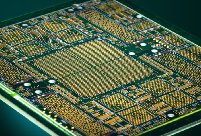
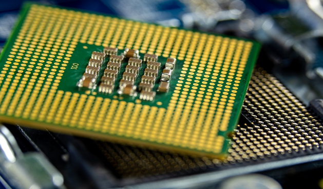
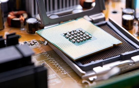
A BGA package differs from conventional IC packaging by replacing the peripheral leads with an array of solder balls arranged in a grid pattern on the underside of the component. These solder balls serve as both electrical connections and mechanical attachments to the printed circuit board. The BGA approach allows for significantly higher pin counts than leaded packages while maintaining a relatively small footprint—a critical advantage in today’s electronics where space constraints are paramount.
The development of BGA technology can be traced back to the 1970s, but it gained widespread adoption in the 1990s as microprocessor and application-specific integrated circuit (ASIC) designs demanded more I/O connections. Since then, BGA packages have evolved into various forms including plastic BGAs (PBGAs), ceramic BGAs (CBGAs), tape BGAs (TBGAs), and micro BGAs (μBGAs), each suited for specific applications and performance requirements.
BGA Package Types and Characteristics
Understanding the different types of BGA packages is essential for selecting the right solution for a particular application. The primary variations include:
Plastic Ball Grid Array (PBGA): The most common and cost-effective BGA type, PBGA packages use a plastic substrate with solder balls typically ranging from 0.45 mm to 1.0 mm in diameter. These packages offer good thermal and electrical performance for most commercial applications and are widely used in consumer electronics, networking equipment, and computer peripherals.
Ceramic Ball Grid Array (CBGA): Featuring a ceramic substrate instead of plastic, CBGAs provide superior thermal conductivity and mechanical stability. The ceramic material allows for higher operating temperatures and better reliability in harsh environments, making these packages ideal for military, aerospace, and high-reliability industrial applications. However, the ceramic substrate increases the package cost significantly compared to PBGAs.
Tape Ball Grid Array (TBGA): TBGA packages utilize a flexible polyimide tape as the substrate material, offering a thin profile and lightweight solution. The tape substrate provides good thermal performance while allowing for some flexibility in the package design. TBGAs are often used in space-constrained applications like mobile devices where thickness is a critical factor.
Micro Ball Grid Array (μBGA): Representing the miniaturization trend in electronics, μBGAs feature extremely fine pitch solder balls (often below 0.5 mm pitch) and compact package sizes. These packages are particularly valuable in portable electronics where board space is at a premium. However, the small size demands precise manufacturing and assembly processes.
Flip Chip BGA (FCBGA): In this advanced configuration, the semiconductor die is mounted upside down (flipped) and connected directly to the substrate using solder bumps. FCBGAs eliminate the need for wire bonds, reducing inductance and allowing for higher-speed operation. These packages are commonly used for high-performance processors, graphics chips, and other demanding applications.
Each BGA variant offers distinct advantages in terms of thermal performance, electrical characteristics, reliability, and cost. Designers must carefully evaluate these factors when selecting a BGA package for their specific application requirements.
BGA PCB Design Considerations
Designing printed circuit boards for BGA components requires careful attention to numerous factors to ensure proper functionality, reliability, and manufacturability. Some of the key design considerations include:
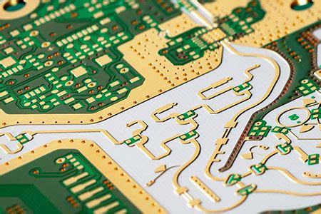
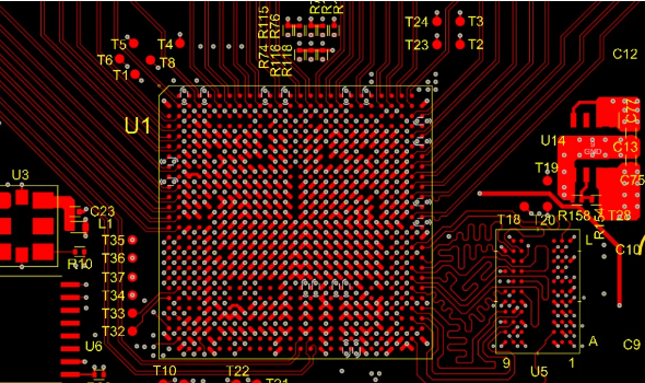
Pad Design and Layout: The PCB land pattern for BGA components must precisely match the package’s ball array. Pad sizes are typically slightly smaller than the solder balls to ensure proper self-alignment during reflow soldering. A common practice is to use non-solder mask defined (NSMD) pads for BGAs, where the copper pad is smaller than the solder mask opening, providing better solder joint reliability.
Via Strategies: Routing signals from BGA components often requires innovative via approaches. For fine-pitch BGAs, designers may use:
- Dog-bone fanout patterns with via-in-pad technology
- Microvias (laser-drilled vias with smaller diameters)
- Blind and buried vias to optimize layer transitions
- Via-in-pad plating fill to create flat surfaces for solder ball attachment
Trace Routing: High-density BGA components demand careful trace routing to maintain signal integrity while accommodating all necessary connections. Key routing techniques include:
- Implementing escape routing patterns that efficiently fan out signals
- Maintaining consistent impedance for high-speed signals
- Properly managing differential pairs and length matching
- Utilizing appropriate layer stackups for optimal signal return paths
Thermal Management: Many BGA packages, especially those housing high-power devices, require careful thermal design. Effective strategies include:
- Incorporating thermal vias beneath the package to conduct heat to inner layers or heatsinks
- Using thermal pads or exposed die paddles for enhanced heat dissipation
- Designing adequate copper pours and heatsink attachment points
- Considering the use of thermal interface materials when necessary
Manufacturing Tolerances: BGA designs must account for PCB fabrication and assembly tolerances, including:
- Solder mask alignment tolerances
- Drilling and plating variations
- Solder paste printing consistency
- Component placement accuracy
Design for Test (DFT): Testing BGA assemblies presents challenges due to the hidden nature of solder joints. DFT considerations include:
- Incorporating test points for critical signals
- Planning for boundary scan (JTAG) testing where applicable
- Considering x-ray inspection requirements
- Providing adequate space for test fixtures
By addressing these design considerations early in the development process, engineers can create BGA PCB designs that are both high-performing and manufacturable, reducing the risk of costly redesigns or production issues.

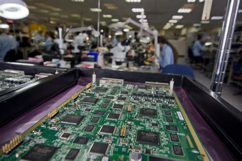
BGA Assembly Processes and Challenges
The assembly of BGA components onto printed circuit boards involves specialized processes that differ significantly from traditional through-hole or surface-mount technologies. Understanding these processes is crucial for achieving high yields and reliable solder joints.
Solder Paste Printing: The first critical step in BGA assembly is applying solder paste to the PCB pads. For BGA components, this typically involves:
- Using fine-pitch stencils with precise aperture designs
- Selecting appropriate solder paste formulations (particle size, flux chemistry)
- Ensuring proper stencil alignment and consistent paste deposition
- Implementing solder paste inspection (SPI) systems to verify print quality
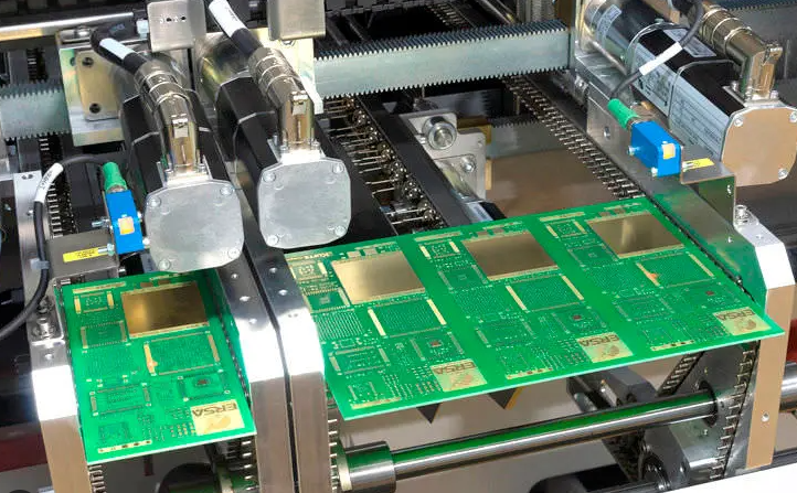
Component Placement: Accurate placement of BGA components is essential for successful assembly. Key aspects include:
- High-precision pick-and-place machines with vision systems
- Careful handling to prevent damage to solder balls
- Proper alignment to ensure all balls contact corresponding pads
- Consideration of thermal expansion effects during placement
Reflow Soldering: The reflow process melts the solder paste and forms permanent connections between the BGA and PCB. Critical parameters include:
- Optimized reflow profiles with appropriate temperature ramps
- Sufficient time above liquidus (TAL) for proper joint formation
- Peak temperature control to prevent component damage
- Nitrogen atmosphere for improved wetting in some applications
Inspection and Testing: Unlike leaded components, BGA solder joints are hidden beneath the package, requiring specialized inspection methods:
- X-ray inspection to examine solder joint quality and voiding
- Automated optical inspection (AOI) for external examination
- Boundary scan testing for electrical verification
- Functional testing to ensure proper operation
Rework Processes: When BGA components need replacement or repair, specialized rework stations are required, featuring:
- Precise local heating systems (typically hot air or IR)
- Vacuum pickup tools for component removal
- Site redressing capabilities (solder removal and cleaning)
- Accurate reballing or replacement procedures
Challenges in BGA Assembly: Several factors can complicate BGA assembly processes:
- Solder Voiding: Entrapped gas bubbles in solder joints can affect thermal and mechanical performance
- Head-in-Pillow Defects: Incomplete merging of solder paste and BGA balls
- Tombstoning: Component misalignment due to uneven heating or solder paste volumes
- Thermal Stress: Mismatched coefficients of thermal expansion (CTE) causing warpage or joint cracking
- Moisture Sensitivity: Many BGA packages require baking before assembly to prevent popcorning
To address these challenges, manufacturers implement various process controls and quality measures:
- Strict moisture control protocols for moisture-sensitive devices
- Advanced process monitoring and statistical process control
- Regular equipment calibration and maintenance
- Comprehensive operator training programs
- Detailed process documentation and work instructions
By understanding and carefully managing these assembly processes and challenges, manufacturers can achieve high yields and reliable BGA assemblies, even with increasingly complex and miniaturized packages.
Reliability Considerations and Failure Modes
Ensuring long-term reliability is paramount when using BGA technology, particularly in mission-critical applications. Understanding potential failure modes and their mitigation strategies is essential for robust design and manufacturing.
Common BGA Failure Modes:
- Solder Joint Fatigue: Cyclic thermal stresses can lead to crack initiation and propagation in solder joints, eventually causing electrical opens. This is particularly problematic in applications with frequent power cycling or environmental temperature variations.
- Thermo-Mechanical Stress: Mismatches in coefficients of thermal expansion (CTE) between the BGA package, solder balls, and PCB can induce significant stresses during temperature changes, potentially leading to joint failure.
- Electromigration: High current density through solder joints can cause metal ion migration, leading to void formation and increased resistance.
- Kirkendall Voiding: Uneven intermetallic compound growth at solder interfaces can create voids that weaken joints.
- Whisker Growth: Spontaneous growth of tin whiskers in lead-free solder alloys may cause short circuits.
- Moisture-Induced Damage: Absorbed moisture in plastic packages can vaporize during reflow, causing delamination or “popcorning.”
Reliability Enhancement Strategies:
- Material Selection: Choosing appropriate solder alloys (e.g., SAC305 for lead-free applications) and underfill materials can significantly improve reliability.
- Underfill Application: For critical applications, epoxy underfill materials can be dispensed beneath BGA components after assembly to distribute stresses and prevent crack propagation.
- Design Optimization: Implementing proper pad geometries, via structures, and board stackups helps manage thermal and mechanical stresses.
- Conformal Coating: Protective coatings can shield BGA assemblies from environmental factors like moisture and contaminants.
- Accelerated Life Testing: Subjecting assemblies to thermal cycling, vibration, and other stress tests helps identify potential reliability issues before field deployment.
Thermal Cycling Reliability:
Thermal cycling tests are particularly important for evaluating BGA reliability. Key parameters include:
- Temperature range (ΔT)
- Cycle frequency and dwell times
- Rate of temperature change
- Number of cycles to failure
Industry standards like JEDEC JESD22-A104 provide guidelines for conducting thermal cycling tests. The results help predict field reliability and compare different package and board configurations.
Mechanical Shock and Vibration Resistance:
BGA assemblies in automotive, aerospace, and portable electronics must withstand mechanical shocks and vibrations. Design strategies to improve mechanical robustness include:
- Using corner bond adhesives for additional mechanical support
- Optimizing board stiffener designs
- Selecting appropriate solder alloys with better mechanical properties
- Implementing proper board mounting and support structures
High-Frequency Performance Considerations:
For high-speed digital or RF applications, BGA interconnects must maintain signal integrity. Critical factors include:
- Controlling impedance through proper via design
- Minimizing discontinuities in signal paths
- Managing return currents through adequate reference planes
- Reducing crosstalk through careful routing and shielding
By addressing these reliability considerations throughout the design and manufacturing process, engineers can develop BGA-based products that meet stringent quality and longevity requirements across various operating environments.
Applications and Future Trends in BGA Technology
BGA technology has become ubiquitous across virtually all sectors of the electronics industry due to its numerous advantages. Current applications and emerging trends demonstrate the continued evolution and importance of this packaging approach.
Current Applications of BGA Technology:
- Computing Hardware:
- Central processing units (CPUs) and graphics processing units (GPUs)
- Chipset components on motherboards
- High-performance memory modules
- Solid-state drive controllers
- Telecommunications:
- Network processors and switches
- Baseband processors in cellular infrastructure
- High-speed transceivers and PHY devices
- Optical networking components
- Consumer Electronics:
- Smartphone application processors
- Tablet and laptop system-on-chip (SoC) devices
- Gaming console main processors
- Smart TV controllers
- Automotive Electronics:
- Advanced driver assistance systems (ADAS)
- Infotainment system processors
- Engine control units (ECUs)
- Autonomous vehicle computing platforms
- Industrial and Medical:
- Programmable logic controllers (PLCs)
- Medical imaging equipment processors
- Industrial automation controllers
- Test and measurement instrumentation
Emerging Trends in BGA Technology:
- Continued Miniaturization:
- Development of even finer pitch BGA variants (below 0.3 mm pitch)
- Ultra-thin BGA packages for wearable devices
- 3D packaging approaches like package-on-package (PoP) configurations
- Advanced Materials:
- Novel substrate materials with improved thermal and electrical properties
- Low-loss dielectric materials for high-frequency applications
- Alternative solder alloys with better reliability characteristics
- Heterogeneous Integration:
- Integration of multiple dies in single BGA packages (2.5D and 3D ICs)
- Silicon interposer technology for high-density interconnects
- Chiplets-based designs using advanced packaging
- Thermal Management Innovations:
- Embedded microchannel cooling solutions
- Integrated heat spreaders and vapor chambers
- Thermally conductive underfill materials
- High-Speed Design:
- Optimization for 112G and higher SerDes interfaces
- Improved power delivery networks for high-current processors
- Advanced signal integrity modeling and analysis techniques
Industry Standards and Developments:
The BGA technology landscape continues to evolve through various industry initiatives:
- JEDEC standards for package qualifications and testing procedures
- IPC guidelines for assembly and reliability requirements
- Development of new package outlines and specifications
- Advancements in design tools and simulation capabilities
Challenges for Future BGA Technology:
As BGA technology pushes into new frontiers, several challenges must be addressed:
- Maintaining solder joint reliability with shrinking geometries
- Managing increasing power densities and thermal loads
- Ensuring manufacturability and yield at scale
- Controlling costs despite increasing complexity
- Addressing environmental and regulatory requirements
The future of BGA technology appears bright, with ongoing innovations ensuring its continued relevance in an electronics industry that demands ever-higher performance in increasingly compact form factors. As system requirements grow more demanding, BGA packaging will likely remain at the forefront of advanced electronic packaging solutions, adapting to meet the needs of next-generation applications from artificial intelligence hardware to quantum computing interfaces.