The Comprehensive Guide to PCB Pads: Design, Types, and Functionality
Introduction to PCB Pads
Printed Circuit Board (PCB) pads are fundamental components of electronic circuit design, serving as the critical connection points between components and the conductive traces on the board. These small but essential features provide both mechanical support and electrical connectivity for electronic components, ranging from simple resistors to complex integrated circuits.
PCB pads have evolved significantly since the early days of electronics. In the 1950s, pads were often hand-soldered points on phenolic boards, while today’s pads are precision-engineered features designed for automated assembly processes. Modern pads must accommodate various component types, soldering techniques, and reliability requirements while minimizing space usage in increasingly compact electronic devices.
The importance of proper pad design cannot be overstated. Well-designed pads ensure:
- Reliable electrical connections
- Strong mechanical bonds
- Efficient manufacturability
- Long-term durability
- Consistent performance across temperature variations and mechanical stress
Basic Pad Types and Their Applications
Through-Hole Pads
Through-hole pads represent one of the oldest and most reliable connection methods in PCB design. These pads feature drilled holes that accommodate component leads which are then soldered on one or both sides of the board.
Key characteristics:
- Hole diameter typically 0.2-0.5mm larger than component lead
- Annular ring (copper surrounding the hole) usually 0.15-0.4mm
- Common in high-reliability applications like military and aerospace
- Suitable for wave soldering processes
Through-hole pads are particularly valued for their mechanical strength, making them ideal for components subject to physical stress such as connectors or large capacitors. However, they consume more board space than surface mount alternatives and require drilling operations that add to manufacturing complexity and cost.
Surface Mount Pads (SMD Pads)
Surface Mount Device (SMD) pads have become the industry standard for most modern electronics due to their space efficiency and compatibility with automated assembly.
Design considerations:
- Pad size matches component termination dimensions
- Solder mask defined or non-solder mask defined configurations
- Thermal relief considerations for heat dissipation
- Alignment with pick-and-place machine requirements
SMD pads enable higher component density and support smaller form factors essential for portable electronics. They also facilitate faster assembly processes since they don’t require drilling and can be placed on both sides of the board.
BGA Pads
Ball Grid Array (BGA) pads present unique challenges in PCB design due to their high density and hidden solder joints beneath the package.
Critical design aspects:
- Precise pad diameter matching ball size (typically 0.2-0.5mm)
- Proper solder mask opening to prevent bridging
- Via-in-pad design considerations
- Escape routing strategies for high pin counts
BGA packages offer significant advantages in terms of pin density and electrical performance but require careful pad design to ensure reliable solder connections that can’t be visually inspected after assembly.
Advanced Pad Structures
Thermal Pads
Thermal pads serve dual purposes: providing electrical connection while managing heat dissipation for components that generate significant thermal energy.
Design features:
- Thermal relief connections to balance heat transfer
- Often connected to large copper areas or ground planes
- May incorporate thermal vias to distribute heat to other layers
- Special considerations for power devices and high-current applications
Proper thermal pad design prevents solder joint issues during reflow while ensuring adequate heat dissipation during operation. These pads frequently appear in voltage regulators, power transistors, and other heat-generating components.
Castellated Pads
Castellated pads, also known as castellations, are plated half-holes along the edge of a PCB that enable module-to-board connections.
Common applications:
- Board-to-board connections
- Module integration (Wi-Fi, Bluetooth modules)
- Edge-mounted components
- Interposers and adapter boards
These specialized pads allow for compact system designs by facilitating vertical stacking of PCBs or the integration of pre-certified modules into larger systems.
Test Pads
Test pads are non-component connection points designed specifically for testing and debugging purposes.
Implementation considerations:
- Size adequate for probe contact (typically 0.5-1mm)
- Spacing for probe access
- Often connected to critical signals
- May include ground reference points
Well-placed test pads significantly improve manufacturability and field serviceability by providing convenient access points for in-circuit testing and diagnostics.
Pad Design Specifications and Standards
IPC Standards for Pad Design
The IPC (Association Connecting Electronics Industries) provides comprehensive standards governing pad design:
Key standards:
- IPC-7351: Generic requirements for surface mount design
- IPC-2221: Generic standard on printed board design
- IPC-SM-782: Surface mount design and land pattern standard
- IPC-7095: Design and assembly process implementation for BGAs
These standards establish guidelines for:
- Pad dimensions relative to component sizes
- Solder joint formation requirements
- Tolerances for manufacturing variations
- Reliability criteria for different product classifications
Manufacturing Considerations
Effective pad design must account for manufacturing capabilities and limitations:
Critical factors:
- Fabrication tolerances (typically ±0.05-0.1mm)
- Solder mask registration accuracy
- Copper etching tolerances
- Drill wander in through-hole applications
- Surface finish characteristics (ENIG, HASL, OSP, etc.)
Designers must understand their manufacturer’s capabilities and design within these constraints to ensure reliable production yields.
Material Considerations
Pad performance depends on material properties:
Key material aspects:
- Copper weight (typically 0.5-2 oz/ft²)
- Surface finish options and their solderability
- Solder mask material and thickness
- Substrate material thermal properties
The choice of materials affects solder joint reliability, electrical conductivity, and long-term durability of the connections.
Pad Design for Manufacturing (DFM)
Solderability Considerations
Proper pad design ensures reliable solder joint formation:
Critical parameters:
- Pad size relative to component termination
- Solder mask clearance
- Thermal balance to prevent tombstoning
- Solder paste volume requirements
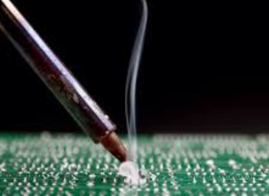
Designs must account for the specific soldering process (wave, reflow, or hand soldering) to achieve consistent, reliable connections.
Assembly Process Compatibility
Pad designs must align with assembly methodologies:
Process-specific considerations:
- Pick-and-place machine accuracy
- Solder paste stencil design
- Reflow profile requirements
- Inspection and testing access
Modern assembly lines require pad designs that accommodate high-speed placement while minimizing defects like bridging or insufficient solder.
Reliability and Durability
Long-term pad performance depends on:
Design factors:
- Mechanical stress relief
- Thermal cycling performance
- Vibration and shock resistance
- Environmental protection requirements
Robust pad designs incorporate features like strain relief, proper copper balancing, and adequate solder volumes to withstand operational stresses over the product lifecycle.
Emerging Trends in Pad Technology
Miniaturization Challenges
Ongoing component shrinkage demands innovative pad solutions:
Current developments:
- Ultra-fine pitch pad designs (below 0.3mm pitch)
- Microvia-in-pad techniques
- Advanced solder mask technologies
- Laser-defined pad geometries
These innovations enable continued progress in electronics miniaturization while maintaining reliability standards.
Advanced Materials
New materials are expanding pad performance boundaries:
Notable advancements:
- Nanocopper surfaces for improved solderability
- Low-temperature solder-compatible finishes
- Conductive adhesives for flexible electronics
- Graphene-enhanced contacts for high-frequency applications
These material developments address challenges in emerging technologies like wearable electronics and high-speed digital systems.
3D and Flexible Electronics
Non-traditional PCB formats require pad innovations:
Adaptation requirements:
- Stretchable interconnects
- Conformal pad designs for curved surfaces
- Anisotropic conductive adhesives
- Flexible substrate compatibility
These specialized pad technologies enable new product categories like flexible displays and conformal sensors.
Conclusion
PCB pads, though small in size, play an outsized role in electronic device functionality and reliability. From basic through-hole connections to advanced BGA implementations, proper pad design remains a cornerstone of successful PCB development. As electronic devices continue evolving toward higher densities, faster speeds, and more demanding operating environments, pad technologies must correspondingly advance to meet these challenges.
The future of pad design will likely see increased automation in design tools, further material innovations, and novel architectures to support emerging electronic applications. However, the fundamental requirements of reliable electrical connection, mechanical stability, and manufacturability will remain constant. By understanding and applying the principles of proper pad design, engineers can ensure their electronic products meet both current requirements and future challenges.